Why immunoscores work in solid tumors—but not yet in blood cancers👇
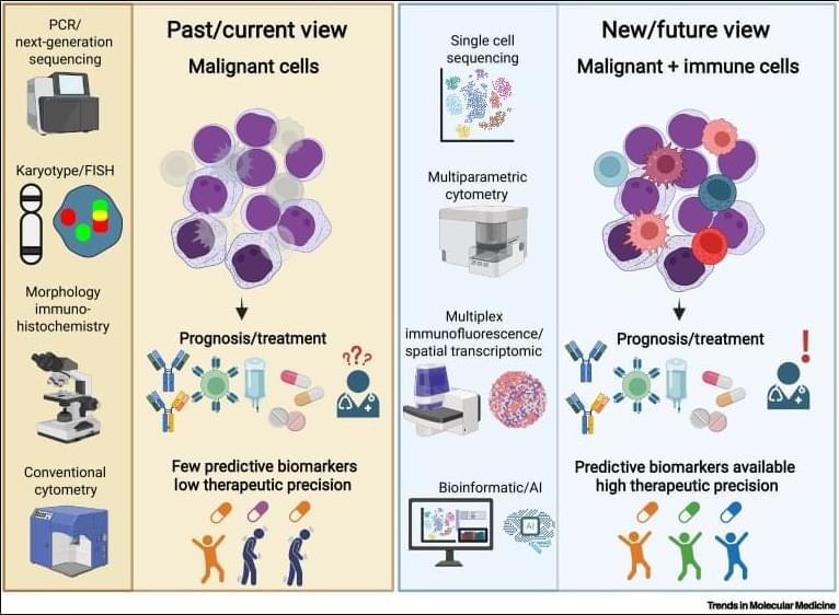
✅In solid tumors, immune profiling has reached a high level of standardization. Clear tumor boundaries allow quantification of immune cell infiltration, particularly CD3⁺ and CD8⁺ T cells, using immunohistochemistry. This has led to the development of validated immunoscores that stratify tumors as “hot,” “cold,” or “very cold,” providing robust prognostic and predictive value for immunotherapy response.
✅These immunoscores work because solid tumors are spatially organized. Immune cells can be classified as infiltrating or excluded, and their density within defined tumor regions directly correlates with clinical outcome. As a result, immune cell infiltration has become a reliable biomarker to guide treatment decisions in cancers such as colon carcinoma.
✅In contrast, hematologic malignancies lack these defining features. Leukemias and lymphomas are systemic diseases without clear tumor borders, making spatial immune assessment fundamentally challenging. Malignant and nonmalignant immune cells coexist within the same compartments, blurring the distinction between tumor cells and the immune microenvironment.
✅Current immune profiling in hematologic cancers relies on baseline physiological levels of circulating or tissue-resident immune cells, including monocytes, neutrophils, T cells, NK cells, and B cells. While techniques such as flow cytometry, histology, and bulk or single-cell RNA sequencing provide rich datasets, they do not yet translate into a unified, clinically actionable immune score.
✅This lack of standardization creates uncertainty in predicting immunotherapy responses. Metrics such as inflammation, cytotoxicity, or immune infiltration are difficult to interpret consistently across patients and disease subtypes, especially given systemic involvement and tissue-specific immune contexts.
💡