Researchers have developed a compact, low-cost convolutional spectrometer that delivers lab-grade precision for applications ranging from industrial quality control to non-invasive health monitoring.
A research team led by Prof. Junghyup Lee of the Department of Electrical Engineering and Computer Science at DGIST has become the first in the world to develop a “time-interleaved noise-shaping SAR ADC (analog-to-digital converter)” semiconductor chip capable of simultaneously measuring multiple biosignals, including electrocardiograms (ECG) and electromyograms (EMG). The team developed this technology in an actual semiconductor chip and successfully completed functional validation. Their findings were presented at the IEEE Symposium on VLSI Technology & Circuits (VLSI 2026), held in Honolulu, June 14–18.
Accurately measuring multiple biosignals using wearable devices such as smartwatches requires meeting several demanding conditions. These include “ultra-high input impedance (resistance)” to prevent signal loss even when no sweat is present on the skin or when contact is loose (dry or non-contact electrodes), a “wide input range” to prevent signal distortion caused by vigorous movement, and “ultra-low power consumption” for long-term operation. However, conventional measurement approaches have struggled to satisfy all these requirements simultaneously within a single chip.
Lee’s research team addressed this challenge by proposing a novel “time-interleaved third-order noise-shaping SAR ADC” architecture in which circuit blocks that consume significant power and chip area are shared across multiple channels, while only essential components (the residual capacitor banks) are allocated separately to each channel. This approach dramatically reduced the circuit area and power consumption required for multichannel systems, enabling an ultra-compact, ultra-low-power chip.
14 years ago, Steve Mann told me that technology that masters nature is not sustainable.
At the time, that sounded like the poetic caution of a man the media had nicknamed “the cyborg Luddite.” Today it reads like a weather report.
Steve is the person the IEEE named the father of wearable computing. He built the EyeTap decades before Google Glass, invented HDR imaging now sitting in the phone in your pocket, and was called the world’s first cyborg. So when he argues for using less, for choosing which technologies to embrace and which to walk away from, he is not speaking from fear of the machine. He is speaking from a deeper intimacy with it than almost anyone alive.
His core move was to refuse the framing everyone else accepted.
Not more technology. Not less technology. Appropriate technology. Balanced with nature instead of replacing it.
And here is the line that has aged into something close to prophecy:
Researchers at Boise State University have developed a novel, environmentally friendly triboelectric nanogenerator (TENG) that is fully printed and capable of harvesting biomechanical and environmental energy while also functioning as a real-time motion sensor. The innovation leverages a composite of Poly (vinyl butyral-co-vinyl alcohol-co-vinyl acetate) (PVBVA) and MXene (Ti3C2Tx) nanosheets, offering a sustainable alternative to conventional TENGs that often rely on fluorinated polymers and complex fabrication.
TENGs are innovative energy-harvesting devices that convert mechanical energy into electricity using the triboelectric effect. They were invented by Prof. Zhong Lin Wang of the Georgia Institute of Technology and generate power through contact and motion between materials, making them ideal for applications like wearable electronics, IoT sensors, and self-powered devices.
This work, published in the journal Nano Energy and led by Ph.D. student Ajay Pratap under the supervision of Prof. David Estrada of the Micron School of Materials Science and Engineering at Boise State University, showcases how additive manufacturing can produce high-performance, skin-compatible, and flexible devices for real-world applications in energy harvesting, wearables electronics, and human-machine interaction.
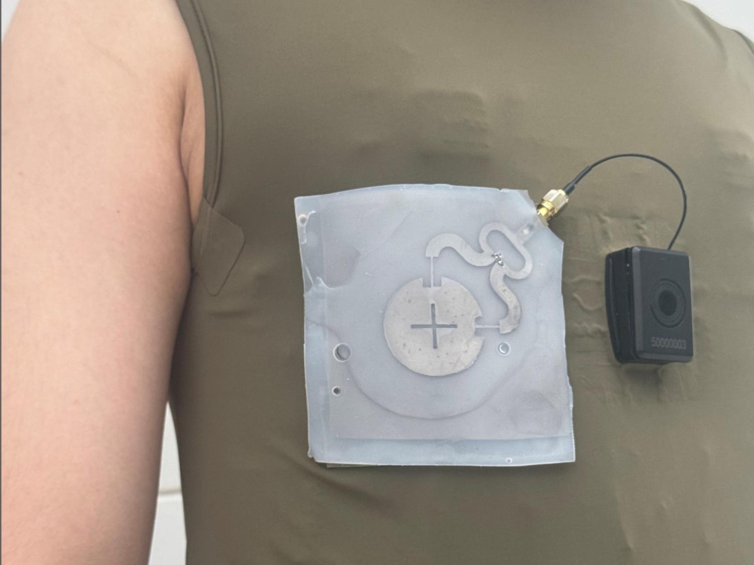
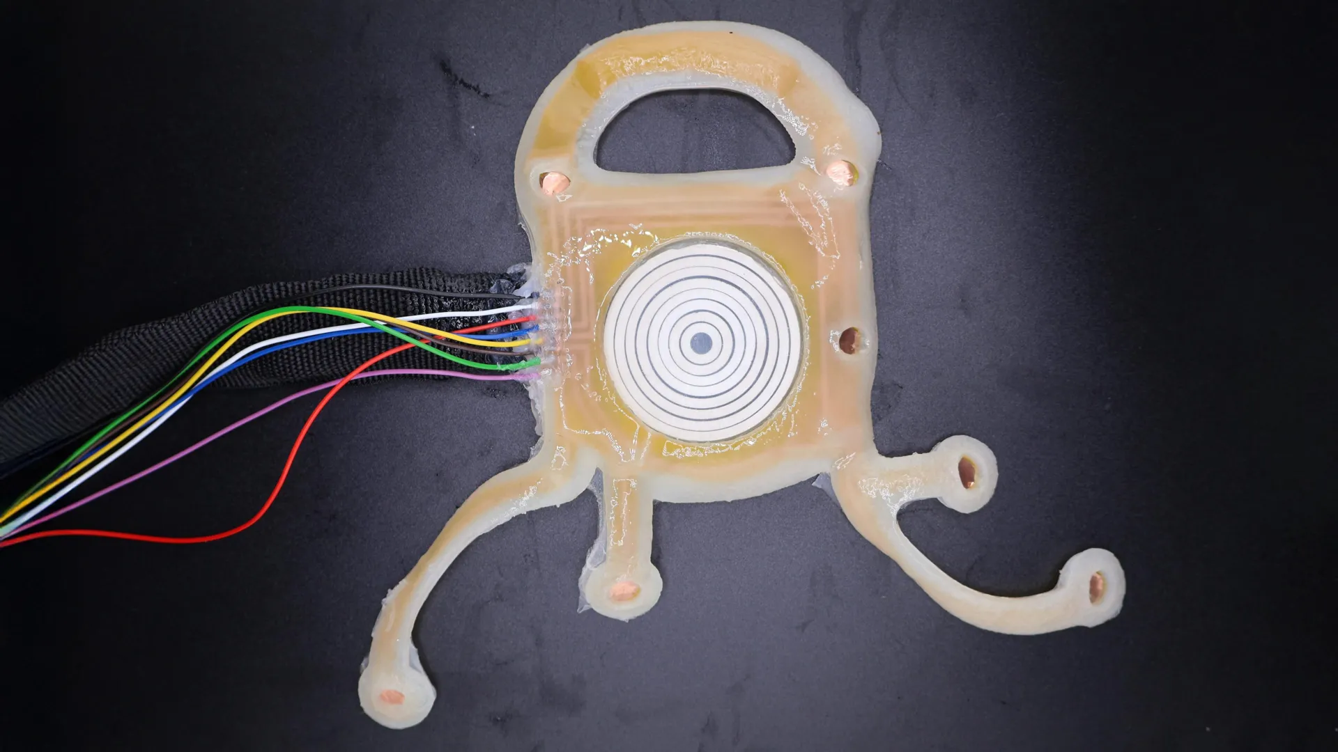
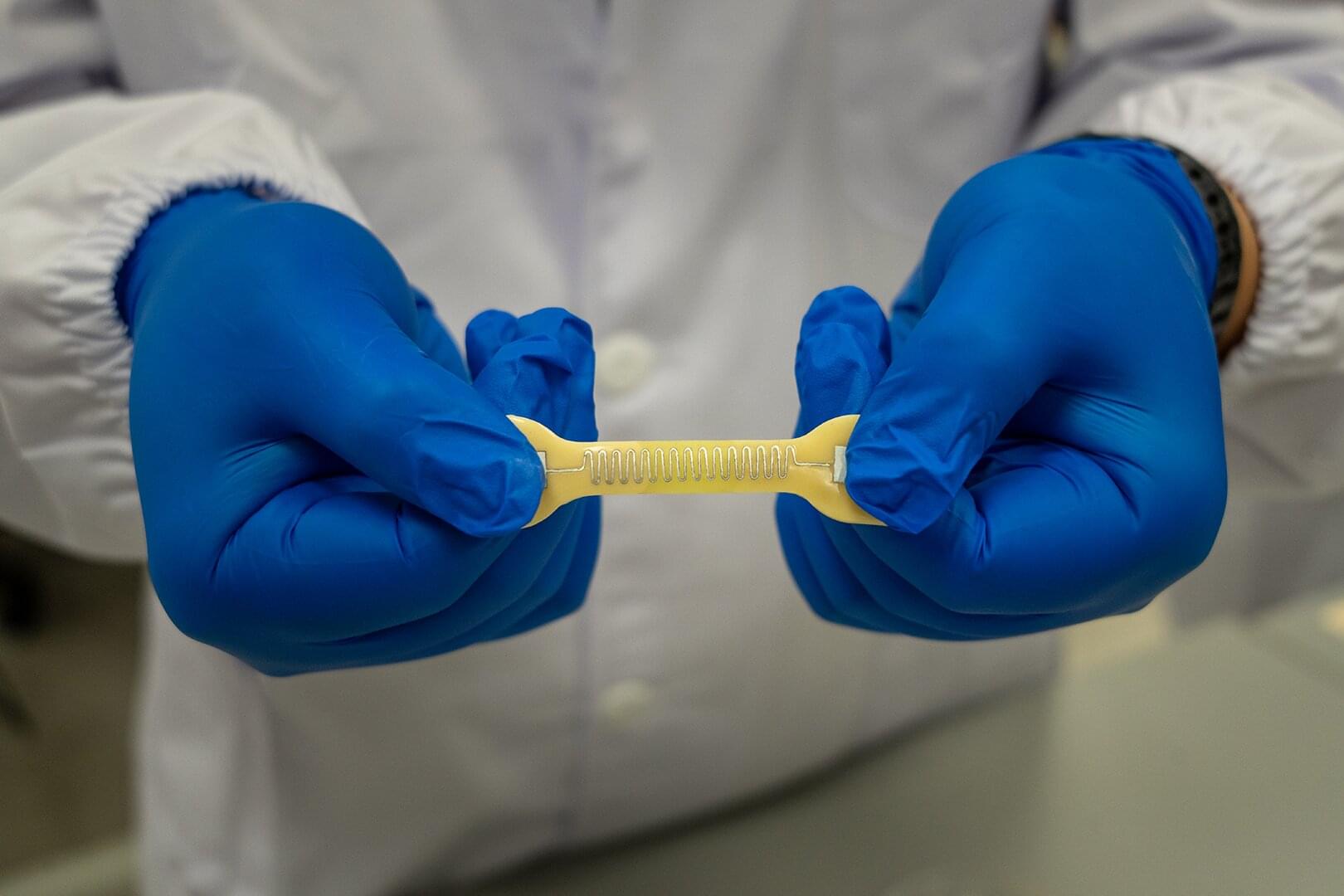
Korean researchers have secured flexible electronic skin technology that can be fabricated directly in the field. This achievement has increased the feasibility of commercializing electronic skin for use in various fields, including robots and wearable devices.
In collaboration with the research team of Professor Ahn Jun Seong from the Department of Control and Instrumentation Engineering at Korea University’s Sejong Campus, the Electronics and Telecommunications Research Institute (ETRI) has developed an in-situ process-based electronic skin fabrication technology capable of producing large-area multimodal sensors without a clean room, a dedicated semiconductor processing facility.
The research is published in npj Flexible Electronics.
In the neonatal intensive care unit, the most fragile patients in medicine are often the most heavily wired. Premature babies, some weighing less than a pound, can be tethered to a tangle of cables, monitors and sensors. Each blood draw to check sugar levels or electrolytes means another needle, another bandage, another moment of stress for an infant whose skin is still forming.
A team of researchers from Tufts University’s Silklab, Helmholtz Munich, Ludwig Maximilian University (LMU) Munich and the Technical University of Munich have developed a radically gentler alternative: a featherlight, silk-based sticker, smaller than a coin, that quietly reads four critical health signals at once just by changing color.
The work, published in ACS Sensors, describes a wearable patch that captures temperature, pH, sodium and glucose from the wisps of fluid that pass naturally through a baby’s still-developing skin. An AI system reads the patch’s color shifts through any standard camera, even in the dim, humid, hard-to-photograph environment of an incubator, and translates them into precise numbers a clinician can act on.
Transistors, small semiconductor-based switches that control the flow of electricity, are central components of all electronic devices, from computers to smartphones, wearables, sensors and smart appliances. Over the past decades, electronics engineers have been continuously working to boost the speed and performance of transistors while also reducing their size.
A promising approach for miniaturizing transistors entails the use of two-dimensional (2D) semiconductors, materials that are only one or a few atoms thick. Despite their potential, most high-performing 2D transistors have so far been demonstrated using relatively wide channels, and it has remained unclear whether their performance can be preserved when the channels are made much narrower.
Researchers at Stanford University recently developed new compact transistors based on narrow strips of monolayer 2D semiconducting materials known as nanoribbons. These transistors, introduced in a paper published in Nature Nanotechnology, were found to perform remarkably well despite their small size, outperforming previously developed nanoribbon transistors based on the same 2D materials.
Researchers at the Medical University of Vienna, in collaboration with ETH Zurich, the Technical University of Munich and Medical Faculty Belgrade, have developed a wearable neurorobotic system that combines electrical neurostimulation with hand exoskeletons. In a clinical trial involving 14 patients with hand impairments caused by neurological injury, the technology supported finger mobility, tactile perception and grip control. The results demonstrate the potential of personalised assistive systems for people living with the consequences of spinal cord or brain injury. The study has recently been published in the journal Science Advances.
Hand movements and the sense of touch are essential for everyday activities such as grasping, eating, dressing or personal hygiene. However, after damage to the central nervous system, motor and sensory impairments of the hand often persist. Conventional rehabilitation can achieve improvements, but does not always lead to sufficient restoration of hand function. There is therefore a great need for assistive technologies suitable for everyday use.
A research team led by study director Stanisa Raspopovic from the Center for Medical Physics and Biomedical Engineering at MedUni Vienna has developed the “SensoExo” system for assisting people with hand sensorimotor impairements. It combines a wearable hand exoskeleton with a custom-fitted neurostimulation sleeve. The sleeve stimulates specific nerves and muscles in the forearm through the skin. Sensors on the fingers detect touch and gripping forces and translate this information into electrical stimulation, providing users with tactile feedback. In addition, functional electrical stimulation can assist users open and close their fingers more easily.
Engineers have invented an ingenious liquid-metal pump that could make future soft robotics and wearable devices much more portable and agile. The innovation, led by the University of Bristol and published in the journal Nature Communications, presents a low-voltage power source with the potential to transform robotic systems for a wide range of applications, from robotic legs to haptic gloves used in medical and industrial settings.
The researchers have demonstrated the varied uses of this innovative technique by creating three prototypes including robotic butterfly wings, a color-changing bracelet, and a haptic fingertip pouch connected to an adjustable wristband which squeezes to simulate natural tactile sensations.w.
Current technologies are powered by bulky compressors or rigid pumps, which limit mobility and flexibility. The small lightweight soft pump—the size of a pea—is powered by liquid metal, which converts electrical energy into fluid motion, creating an efficient, compact power source for next-generation soft robots and adaptive materials such as medical devices and wearable interfaces for virtual reality.
Researchers from the University of Cambridge and GlitterinTech, a startup founded by the same research group, have unveiled a fundamentally new type of optical spectrometer that delivers laboratory-grade precision in a device small enough to be embedded in portable and wearable technologies. By rethinking how spectra are measured and processed, the team has demonstrated a spectrometer costing only around $10, operating at a centimeter scale, and capable of applications ranging from industrial quality control to real-time health care monitoring.
Optical spectrometers underpin countless technologies, from chemical analysis and manufacturing to environmental sensing and medicine. Yet shrinking these instruments has historically involved painful trade-offs: Miniaturized devices typically sacrifice bandwidth, resolution or accuracy, limiting them to rough identification rather than true metrological measurements. The newly reported convolutional spectrometer overcomes these barriers by introducing a conceptually elegant operating principle grounded in the convolution theorem, offering unprecedented performance metrics compared with existing dispersive, Fourier-transform and reconstructive spectrometers.