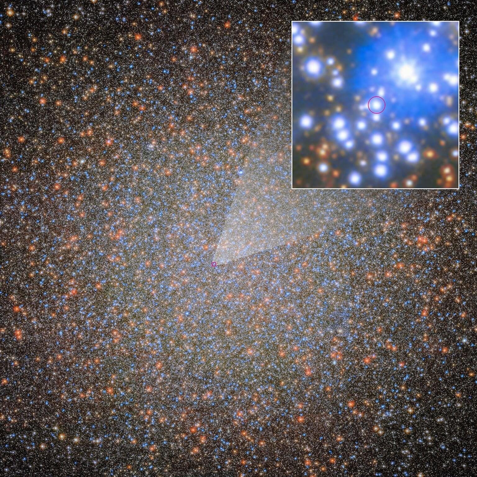
Calculations explain curious properties of some 2D materials
Physicist Davide Bossini from the University of Konstanz has recently demonstrated how to change the frequency of the collective magnetic oscillations of a material by up to 40%—using commercially available devices at room temperature.
“We now have a full picture,” Bossini says. For years, the physicist from the University of Konstanz has studied how to use light to control the collective magnetic oscillations of a material—known as magnons. In the summer of 2025, he was finally able to show how to change the “magnetic DNA” of a material via the interaction between light and magnons.
He now demonstrates how the frequency of oscillations can be controlled quasi instantly and on demand by means of a weak magnetic field and intense laser pulses. In this way, he can increase or decrease frequencies by up to 40%. The effect is due to the interaction of the optical excitation, magnetic anisotropy (directional dependence) and the external magnetic field.
Researchers have shown that consumer-grade 3D printers and low-cost materials can be used to produce multi-element optical components that enable super-resolution imaging, with each lens costing less than $1 to produce. The new fabrication approach is poised to broaden access to fully customizable optical parts and could enable completely new types of imaging tools.
“We created optical parts that enable imaging of life’s smallest building blocks at a remarkable level of detail,” said lead author Jay Christopher from the University of Strathclyde in the UK. “This approach opens the possibility for customized imaging systems and unlocks imaging scenarios that are traditionally either impossible or need costly glass manufacturing services.”
In the journal Biomedical Optics Express, the researchers describe their lens design and manufacturing processes, which combine 3D printing, silicone molding and a UV curable clear resin. They used lenslets fabricated with their technique to create a multifocal structured illumination microscope that imaged microtubules in a cell’s cytoskeleton with a resolution of around 150 nm.
In recent years, electronics engineers have been trying to identify semiconducting materials that could substitute for silicon and enable the further advancement of electronic devices. Two-dimensional (2D) semiconductors, such as molybdenum disulfide (MoS₂), have proved to be among the most promising solutions, as their thinness and resistance to short-channel effects could yield highly performing and smaller electronics.
To create transistors and other electronic components based on 2D materials, however, engineers need to be able to attach electrical connections to them and reliably form ohmic contacts, which allow electrical current to flow freely through the resulting devices. As devices get smaller, however, they also require smaller contacts that have proved to be very difficult to attach to 2D semiconductors.
Researchers at Nanjing University and other institutes in China recently introduced a new strategy to reliably grow ultra-short and low-resistance semimetallic antimony crystal contacts directly on MoS₂
A standard reference thermoelectric module (SRTEM) for objectively measuring thermoelectric module performance has been developed in Korea for the first time. A research team led by Dr. Sang Hyun Park at the Korea Institute of Energy Research developed the world’s second standard reference thermoelectric module, following Japan, and improved its performance by more than 20% compared with existing modules, demonstrating the excellence of Korea’s homegrown technology. The findings are published in the journal ACS Applied Materials & Interfaces.
A thermoelectric module is a device that generates electricity by creating a flow of electrons driven by a temperature difference, with one side becoming cold and the other becoming hot. Conversely, when an electric current is applied to a thermoelectric module, one side cools down while the other side heats up.
Thanks to these characteristics, thermoelectric modules are widely used in applications such as compact camping refrigerators and electronic equipment including computers. In addition, because they are environmentally friendly and well suited to miniaturization, they can be broadly applied to emerging fields such as carbon-free power generation and the space industry, which have recently drawn significant attention.
University of Toronto researchers have designed a new composite material that is both very light and extremely strong—even at temperatures up to 500 Celsius.
The material, which is described in a paper published in Nature Communications, is made of various metallic alloys and nanoscale precipitates, and has a structure that mimics that of reinforced concrete—but on a microscopic scale.
These properties could make it extremely useful in aerospace and other high-performance industries.
A solution to a tricky groundwater riddle from Australia: Researchers at TU Wien have developed numerical models to simulate the movement of fluids in porous materials.
Things are complicated along the Murray–Darling River in southern Australia. Agricultural irrigation washes salt out of the upper soil layers, and this salt eventually ends up in the river. To prevent the river’s salt concentration from rising too much, part of the salty water is diverted into special basins.
Some of these basins are designed to let the salty water evaporate, others to slowly release it in a controlled manner in the underground. That keeps salt temporarily out of the river and allows better management of the river’s water—but it increases the salinity in the ground. How can we calculate how this saltwater spreads underground and what its long-term effects will be?
A textbook rule for the relationship between the structure and strength of a material breaks down for high-speed deformations, like those caused by strong impacts.
On the microscale, metallic materials are made of homogeneous crystalline regions—grains—separated by disordered boundaries. In general, materials with smaller grains are stronger because they have more grain boundaries, which impede deformation. But researchers have now demonstrated a radical departure from this rule: With rapid deformation, such as that from an explosive impact, finer grained metals are softer, not harder [1]. This new insight, the researchers hope, could be useful for engineers developing impact-resistant alloys for armor, aerospace structures, or hypersonic vehicles.
The yield strength of a material is the stress (force) at which it begins to deform permanently rather than springing back. At the atomic scale in crystalline materials, this deformation occurs when sections of the crystal slide past one another, facilitated by the motion of structural defects called dislocations. But at grain boundaries, dislocations are halted and can pile up, which translates into resistance to deformation and increased yield strength. Materials with smaller grains have more grain boundaries than those with larger grains, so smaller grains are associated with higher strength.
Glassy materials are everywhere, with applications far exceeding windowpanes and drinking glasses. They range from bioactive glasses for bone repair and amorphous pharmaceuticals that boost drug solubility to ultra-pure silica optics used in gravitational-wave detectors. In principle, any substance can become glass if its hot liquid is cooled fast enough to avoid forming an ordered crystal.
A distinguishing feature of glass is that its atoms freeze into an irregular, disordered arrangement. This stands in contrast to crystals, where atoms sit in a regular pattern. This disorder gives glass many of its unique and useful properties, but scientists still struggle to understand how atomic-scale disorder produces the properties observed in everyday glasses.