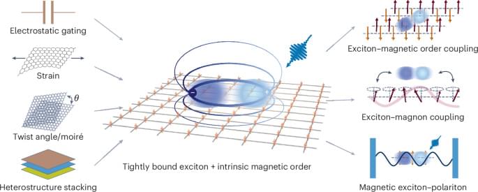
Menu

Blog

Archive for the ‘materials’ category: Page 4

Sep 26, 2024

Researchers develop new p-type semiconductor materials for next-gen displays

Posted by in categories: computing, materials

A group of Korean researchers have recently succeeded in developing new p-type semiconductor materials and thin-film transistors that will lead the innovation of the semiconductor industry. These new discoveries are expected to be widely utilized to improve the overall performance of next-gen displays and ultra-low power semiconductor devices.

Sep 25, 2024

Microchip Breakthrough: This New Material Will Change Everything

Posted by in categories: computing, materials

The first 200 of you will receive the first month of a Planet Wild membership from me for free. Click on this link https://planetwild.com/r/anastasiinte… use the code ANASTASI29 later. You can cancel at any time. If you want to see how Planet Wild works first, check out their latest YouTube video link https://planetwild.com/r/anastasiinte

The video I mentioned about NVIDIA:
➜ • New Nvidia Chip Has a HUGE Problem.

Continue reading “Microchip Breakthrough: This New Material Will Change Everything” »

Sep 25, 2024

Danish physicists make monumental quantum mechanics discovery

Posted by in categories: materials, quantum physics

The research was conducted at the Danish National Research Foundation’s “Center of Excellence for Hybrid Quantum Networks (Hy-Q)” and is a collaboration between Ruhr University Bochum in Germany and the University of Copenhagen’s Niels Bohr Institute.

Note: Materials provided above by the The Brighter Side of News. Content may be edited for style and length.

Sep 23, 2024

Water-free manufacturing approach could help advance 2D electronics integration

Posted by in categories: life extension, materials

The future of technology has an age-old problem: rust. When iron-containing metal reacts with oxygen and moisture, the resulting corrosion greatly impedes the longevity and use of parts in the automotive industry. While it’s not called “rust” in the semiconductor industry, oxidation is especially problematic in two-dimensional (2D) semiconductor materials, which control the flow of electricity in electronic devices, because any corrosion can render the atomic-thin material useless. Now, a team of academic and enterprise researchers has developed a synthesis process to produce a “rust-resistant” coating with additional properties ideal for creating faster, more durable electronics.

The team, co-led by researchers at Penn State, published their work in Nature Communications (“Tailoring amorphous boron nitride for high-performance two-dimensional electronics”).

These materials are made from molybdenum disulfide, a two-dimensional semiconductor, grown on a sapphire surface. The triangular shapes seen are aligned because of a special process called epitaxy, where the material follows the pattern of the surface it’s grown on. Insulating layers, like amorphous boron nitride, are added during the process of making these ultra-thin materials, which are used to build next-generation electronic devices. (Image: J.A. Robinson Research Group/Penn State)

Sep 23, 2024

Analyzing Friction in Layered Materials

Posted by in categories: materials, particle physics

Experiments reveal the factors that determine the friction between the single-atom-thick layers in van der Waals materials, which may have uses in lubrication technology.

Van der Waals (vdW) materials consist of stacked, single-atom-thick layers, and these layers can experience very low friction as they slide over one another, a property that might be exploited for lubrication. A research team has now distinguished several contributions to this low friction and has shown that effects at the edges of the sliding regions dominate [1]. Some of their experiments involved sliding a several-layer-thick flake across a surface made of a similar material containing a crack, which allowed the team to systematically control the edge length. The findings could guide efforts to engineer controllable frictional forces into such materials in micromechanical devices.

The very low friction, called superlubricity, exhibited by vdW materials has been previously shown to depend on the relative orientations of the layers. If one layer is rotated by some angle, called the twist angle, with respect to the layer below, the two layers form a “superlattice” in which the two atomic lattices fall periodically in and out of registry, like a pair of overlaid combs with slightly different spacings. This arrangement is called a Moiré pattern, and the repeating elements, or unit cells, of the superlattice are called Moiré tiles. Superlubricity arises because, in general, the contributions to the frictional force from the atoms within one Moiré tile cancel each other out: Some exert a push, while others exert a pull.

Sep 21, 2024

‘Brain-breaking’ glass bricks are 3D printed, reusable, and strong

Posted by in categories: materials, neuroscience

Using a 3D printer that works with molten glass, researchers forged LEGO-like glass bricks with a strength comparable to concrete. The bricks could have a role in circular construction in which materials are used over and over again.

“Glass as a structural material kind of breaks people’s brains a little bit,” says Michael Stern, a former MIT graduate student and researcher in both MIT’s Media Lab and Lincoln Laboratory. “We’re showing this is an opportunity to push the limits of what’s been done in architecture.”

Continue reading “‘Brain-breaking’ glass bricks are 3D printed, reusable, and strong” »

Sep 21, 2024

This Powerful Nano Disk Could Revolutionize How We Manipulate Light

Posted by in categories: materials, nanotechnology

Researchers have created a disk-like nanostructure that dramatically improves light frequency conversion efficiency. This innovation in photonics combines material and optical resonances in a compact form, paving the way for advanced optical and photonic applications.

Scientists at Chalmers University of Technology, in Sweden, have for the first time succeeded in combining two major research fields in photonics by creating a nanoobject with unique optical qualities. Since the object is a thousand times thinner than a human hair, yet very powerful, the breakthrough has great potential in the development of efficient and compact nonlinear optical devices. “My feeling is that this discovery has a great potential,” says Professor Timur Shegai, who led the study at Chalmers.

Harnessing Light With Advanced Photonics.

Sep 21, 2024

Organic thermoelectric device can harvest energy at room temperature

Posted by in categories: energy, materials

Researchers have developed a new organic thermoelectric device that can harvest energy from ambient temperature. While thermoelectric devices have several uses today, hurdles still exist to their full utilization. By combining the unique abilities of organic materials, the team succeeded in developing a framework for thermoelectric power generation at room temperature without any temperature gradient.

Their findings were published in the journal Nature Communications.

Thermoelectric devices, or thermoelectric generators, are a series of energy-generating materials that can convert heat into electricity so long as there is a —where one side of the device is hot and the other side is cool. Such devices have been a significant focus of research and development for their potential utility in harvesting from other energy-generating methods.

Sep 20, 2024

Infinity on Instagram: ‘Graphene’

Posted by in category: materials

2 likes, — infinitywithoutend on July 21, 2024: ‘Graphene’

Sep 20, 2024

Potential and challenges of computing with molecular materials

Posted by in categories: computing, materials

Molecular materials for computing progress intensively but the performance and reliability still lag behind. Here the authors assess the current state of computing with molecular-based materials and describe two issues as the basis of a new computing technology: continued exploration of molecular electronic properties and process development for on-chip integration.

Page 4 of 29512345678Last