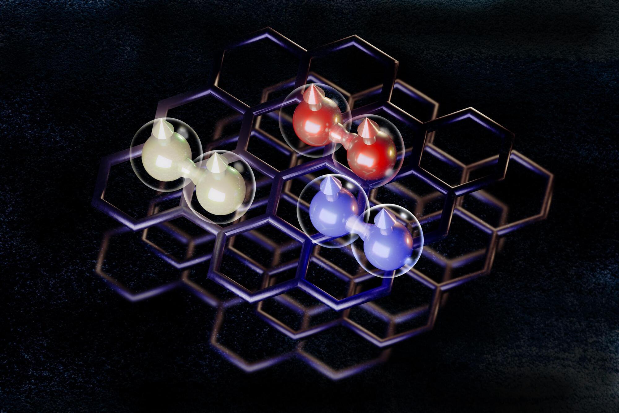
The researchers discovered the multiple superconducting states in atomically thin exfoliations of graphite, known as graphene. Specifically, graphene is a single-atom-thin sheet of carbon atoms arranged precisely in a microscopic lattice. The team made its discoveries in samples of rhombohedral graphene, which is a natural structure within graphite consisting of a stack of four or five graphene layers.
Interestingly, the researchers found that several of the new superconducting states in rhombohedral graphene are able to persist in the presence of a magnetic field, which normally kills superconductivity.
And in a further surprise, these superconducting states even get stronger when exposed to a magnetic field.
Materials called relaxor ferroelectrics have been used for decades in technologies like ultrasounds, microphones, and sonar systems. Their unique properties come from their atomic structure, but that structure has stubbornly eluded direct measurement.
Now a team of researchers from MIT and elsewhere has directly characterized the three-dimensional atomic structure of a relaxor ferroelectric for the first time. The findings, reported today in Science, provide a framework for refining models used to design next-generation computing, energy, and sensing devices.
“Now that we have a better understanding of exactly what’s going on, we can better predict and engineer the properties we want materials to achieve,” says corresponding author James LeBeau, MIT’s Kyocera Professor of Materials Science and Engineering. “The research community is still developing methods to engineer these materials, but in order to predict the properties those materials will have, you have to know if your model is right.”
In 2023, researchers at MIT and Harvard showed that ordinary cement, water, and a small amount of carbon black can be combined into a material that stores electricity, not in a battery embedded in the structure, but in the hardened concrete itself. As the cement hydrates, it consumes water and leaves a network of fine pores behind. The hydrophobic carbon black migrates into these spaces and self-assembles into a percolating, fractal-like electron-conducting network threaded through the calcium-silicate-hydrate (C-S-H) matrix. Soaked in an electrolyte and paired across a thin separator, two such electrodes form an electric double-layer capacitor, a supercapacitor, that stores charge electrostatically across an enormous internal surface area. The more interfacial surface inside the block, the more charge it holds. By the researchers’ calculation, a foundation-scale block of roughly 45 cubic metres, a cube about 3.5 metres across, could store on the order of 10 kilowatt-hours, comparable to a household’s average daily electricity use, while still bearing structural load. A 2025 follow-up reported a roughly tenfold increase in energy density, shrinking the volume needed for the same storage. This remains laboratory-scale work, demonstrated so far in small cells and prototypes, not a deployed foundation. Open questions include cycle life, self-discharge, and real-world scaling. References Chanut, N., Stefaniuk, D., Weaver, J. C., Zhu, Y., Shao-Horn, Y., Masic, A., & Ulm, F.-J. (2023). Carbon–cement supercapacitors as a scalable bulk energy storage solution. Proceedings of the National Academy of Sciences, 120(32), e2304318120. Stefaniuk, D., Weaver, J. C., Ulm, F.-J., & Masic, A. (2025). High energy density carbon–cement supercapacitors for architectural energy storage. Proceedings of the National Academy of Sciences, 122(40), e2511912122. PHENOMICA — contemplative, precise science, one phenomenon at a time. #science #materialscience #supercapacitor #energystorage #concrete …
More accurate navigation systems and improved wireless communications may not come from traditional electronics, but rather from atoms. Researchers at Penn State and the National Institute of Standards and Technology (NIST) have developed a new way to build tinier, smarter glass sensors filled with highly precise and stable atoms.
The team’s work, published this week (June 18) in Microsystems and Nanoengineering, centers on a manufacturable, silicon-free version of traditional bulky “vapor cells”—sealed chambers that contain cesium and rubidium atoms—that are commonly used in precision measurement systems, in a gas state. These atoms can act as highly precise sensors because, unlike manufactured components, atoms are fundamentally identical.
“Using atoms for sensing is advantageous because the physics of individual atoms is very well understood, and all the atoms are equal,” said Daniel Lopez, co-lead author of the paper, Liang Professor of Electrical Engineering and Computer Science at Penn State and director of the Nanofabrication Lab at the Materials Research Institute (MRI). “That gives you a level of precision that’s very hard to achieve with traditional microfabricated devices.”
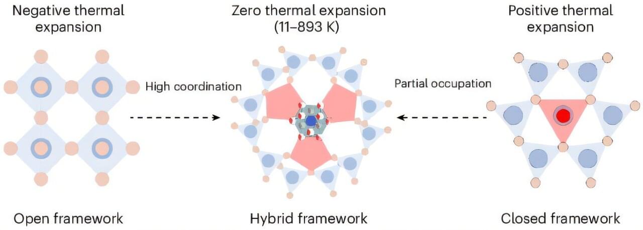
Almost every material expands when heated. Well-known examples include railroad tracks and concrete roadways, which feature visible expansion gaps to accommodate this effect. However, thermal expansion poses a far more acute challenge for extremely precise technologies, such as lasers and semiconductor manufacturing equipment, where even minute dimensional changes can compromise precision.
Scientists have long sought to develop materials that maintain dimensional stability across a wide temperature range.
Now, a team led by Prof. Lin Zheshuai from the Technical Institute of Physics and Chemistry (TIPC) of the Chinese Academy of Sciences (CAS) has designed a material with an exceptionally broad zero-thermal-expansion temperature window.
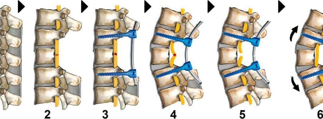
In humans and other mammals, spinal cord injuries can be devastating, leading to permanent loss of movement, sensation and bladder control. When severed axons (the long fibers that carry messages between nerve cells) cannot regrow, a dense scar forms, preventing nerve signals from passing the injury site.
But the situation is different for some primitive invertebrates, which can rapidly reconnect severed nerves by fusing them. Inspired by this natural phenomenon, scientists led by Michael Lebenstein-Gumovski at the Sklifosovsky Institute for Emergency Medicine in Russia report that they have successfully reconnected severed spinal cords in pigs, enabling them to walk again.
When a spinal cord is completely cut, the two severed ends naturally pull away from each other. In microscopic roundworms, for example, the nerve ends automatically find each other and fuse together. The researchers realized that to recreate a natural fusion process like this, they needed a material to fill the empty space and hold the two ends together.
The field of magnonics aims to take advantage of spin waves, which are waves of precessing spins that can propagate in certain magnetic materials. A spin wave containing many equally spaced frequencies—called a magnon frequency comb (MFC)—would be especially useful for information processing and magnetic-field detection. Unfortunately, generating such waves is complicated. Now Peng Yan and his colleagues at the University of Electronic Science and Technology of China have shown theoretically that MFCs could be produced by simply creating a tiny bump in a thin magnetic layer [1].
Creating an MFC in a magnetic material usually entails creating an intricate pattern or “texture” of spin orientations in a small region—such as a spin vortex—and irradiating those spins with monochromatic microwaves. To avoid the complexities of spin textures, Yan and his colleagues propose introducing a bump in a few-nanometer-thick magnetic film. Previous research showed that material curvature can affect spin waves, for example, by modifying the frequency–wavelength relationship.
Exploiting another curvature effect, the theorists showed that a bump between 4 and 64 nm high can spontaneously create a set of spin waves that remain restricted to the bump region. Irradiating the bump with microwaves of a specific frequency then excites these waves and launches an MFC that travels away from the bump. Adjusting the height of the bump changes the spacing of the comb frequencies. Team member Hao Zhao says that in addition to possibly making MFCs more widely available, the work shows the potential for using geometry to manipulate spin waves in new ways.
Sound waves, light waves and other types of waves, generally spread freely through space and over time. In 1958, physicist Philip W. Anderson first described a phenomenon via which irregularities or other sources of disorder in materials would prevent waves from propagating freely, which is now known as Anderson localization.
In quantum systems, one can observe quantum states that are spread throughout a system (i.e., extended), confined to a small region (i.e., localized) or somewhere between the two (i.e., critical). Critical quantum states have so far proved to be very difficult to identify and study using Anderson’s localization theory.
Researchers at the International Quantum Academy and Southern University of Science and Technology in China recently set out to further explore critical quantum states in a quantum processor based on superconducting qubits.