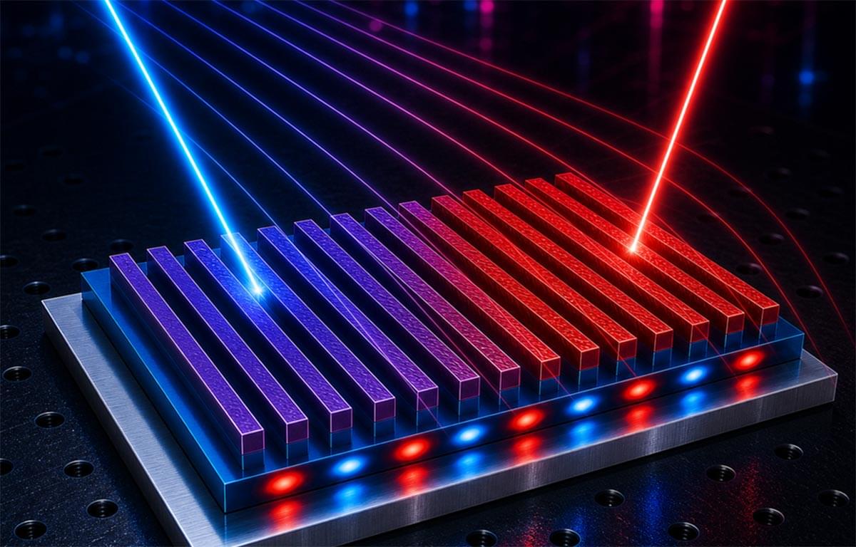
Scientists have created a programmable material that gives engineers unprecedented control over heat, with potential applications ranging from energy systems to next generation photonic memory.
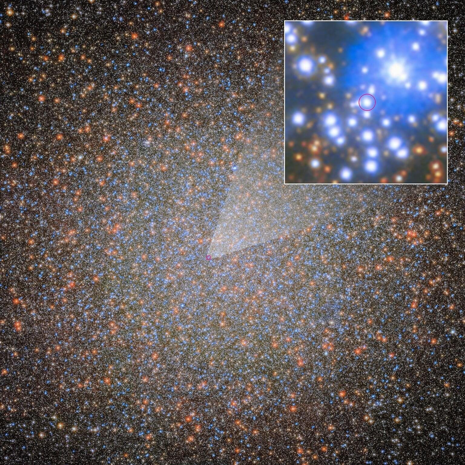
The massive globular star cluster Omega Centauri has puzzled astronomers for decades. It should be filled with black holes left behind by exploding stars, yet evidence for them is scarce. Now, astronomers using archival data from NASA’s Hubble Space Telescope and supporting observations from NASA’s James Webb Space Telescope have finally located the first stellar-mass black hole in this cluster. Discovering the first of this missing black hole population will help refine current theories on black hole formation within environments such as Omega Centauri. The team’s findings were published in The Astrophysical Journal Letters.
Omega Centauri consists of 10 million gravitationally bound stars. Though the astronomical community previously found evidence using Hubble that an intermediate-mass black hole lurks at its center, models suggest this star cluster should also contain about 10,000 smaller, stellar-mass black holes. This notable population of black holes evaded detection in previous observational studies, which used the radial velocity method or looked for radio and X-ray emission from material falling onto black holes.
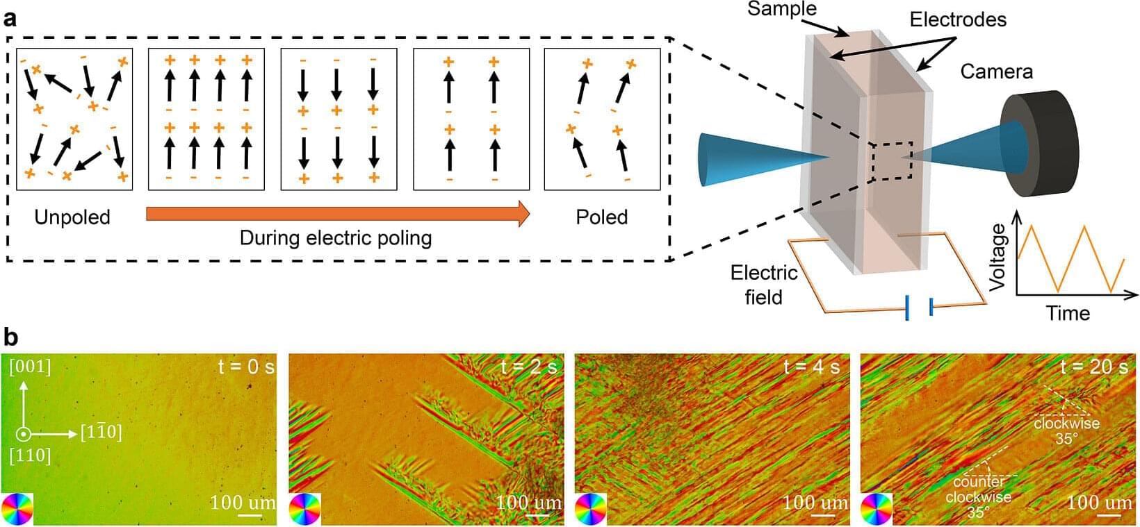
New research is shedding light on longstanding debates over the behavior of ferroelectric materials when those materials are exposed to electric fields. The findings stem from the use of a novel technique that allows researchers to observe the real-time behavior of domain walls in ferroelectric materials as they are “poled” and “depoled.”
Ferroelectric materials are used in a wide range of technologies, from sensors to actuators, and their electrical properties are critical to their utility. It’s well established that you can bring the various domains in a ferroelectric material into alignment by applying an electric field—either direct current (DC) or alternating current (AC). This is called “poling.” However, there has been significant debate about what exactly is taking place during the poling process.
“We’re now able to observe what is happening in real time, which gives us deeper insights into the mechanisms at play—which will inform our ability to engineer materials in order to produce the electrical characteristics we’re looking for,” says Jun Liu, co-corresponding author of two papers on the work and an associate professor of mechanical and aerospace engineering at North Carolina State University.
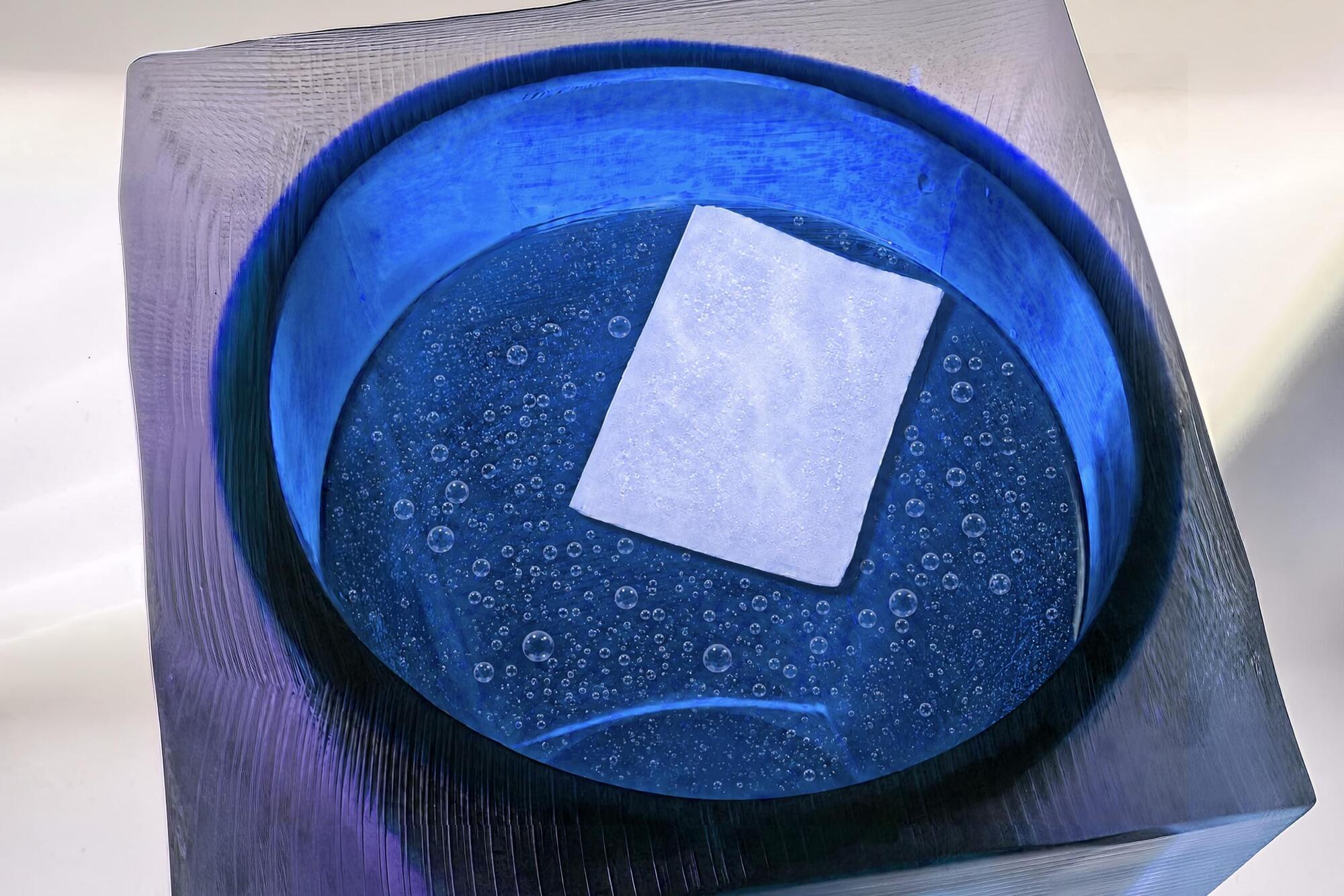
For all their sticky, stretchy, and protective properties, hydrogels lack one key trait: breathability. If worn for too long, a bandage or patch can trap moisture and sweat, which can irritate tissues and reduce the effectiveness of any device that a hydrogel adheres.
Now MIT engineers have come up with a recipe for a hydrogel that is both hydrated and aerated, or permeable to air. The new material is just as soft, stretchy, and robust as conventional hydrogels, but a network of tiny tunnels running through the gel allows air to pass through.
The aerated hydrogel can be worn for longer periods of time compared to conventional hydrogels, without causing skin irritation. It can also reduce sweat buildup, even during exercise. In experiments, volunteers wore wireless heart monitors that were attached to their chest with the new breathable hydrogel. After working out regularly for 10 days, the volunteers showed no signs of skin irritation, and the heart monitors maintained clear readings.

Advanced magnetic memory and spintronic devices rely on the ability to control magnetic states using electricity. Today, such technologies work by manipulating relatively simple magnetic structures found in ferromagnets, where all the magnetic moments point the same way. However, researchers are becoming increasingly interested in controlling more complex magnetic systems because these could offer higher information density and improved efficiency.
Helimagnets are a prime example of such systems. In these materials, the magnetic moments form spiral or helical patterns that wind through the material. The direction in which these magnetic patterns propagate plays an important role in determining the material’s electrical and magnetic behavior.
However, researchers had not established a reliable way to reversibly control the orientation of helical magnetic structures using an electric current, and current-driven techniques developed for ferromagnets do not directly carry over to helimagnetic systems.
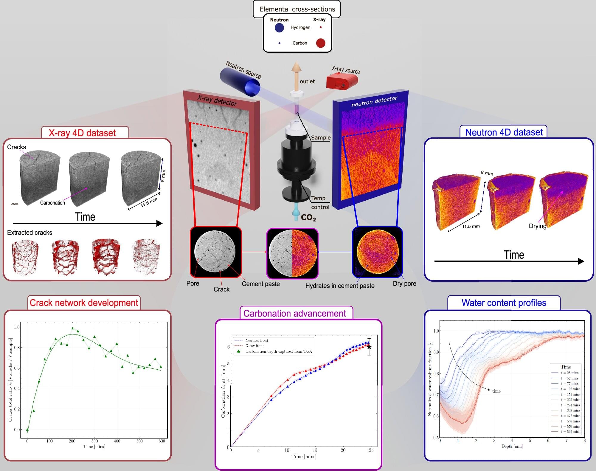
The construction sector faces two problems at once: it emits large amounts of CO₂ and produces vast quantities of concrete waste. But what if part of that waste could be used to trap carbon instead of ending up as rubble?
That is the idea behind accelerated carbonation.
Crushed recycled concrete can be exposed to CO₂-rich gas, allowing carbon dioxide to react with the old cement paste and become locked into stable mineral compounds. In principle, this could help reduce the environmental impact of construction while giving demolition waste a second life.
The work lays the foundation to build a new platform to explore phenomena that could power devices capable of transporting and grouping electrical signals and quantum states in ways not traditionally achievable without relying on optical or engineered systems. The team detailed its findings in a paper published in Science Advances.
Non-Hermitian physics refers to systems that exhibit behaviors not found in conventional physical models, explained Morteza Kayyalha, assistant professor of electrical engineering at Penn State and corresponding author on the paper. These systems can display unusual behaviors, such as enhanced responses to perturbations and external stimuli. They can also demonstrate the non-Hermitian skin effect, where quantum states—which researchers can use to predict the physical properties of a material—become concentrated near a specific boundary or point in the material, rather than spreading uniformly throughout.
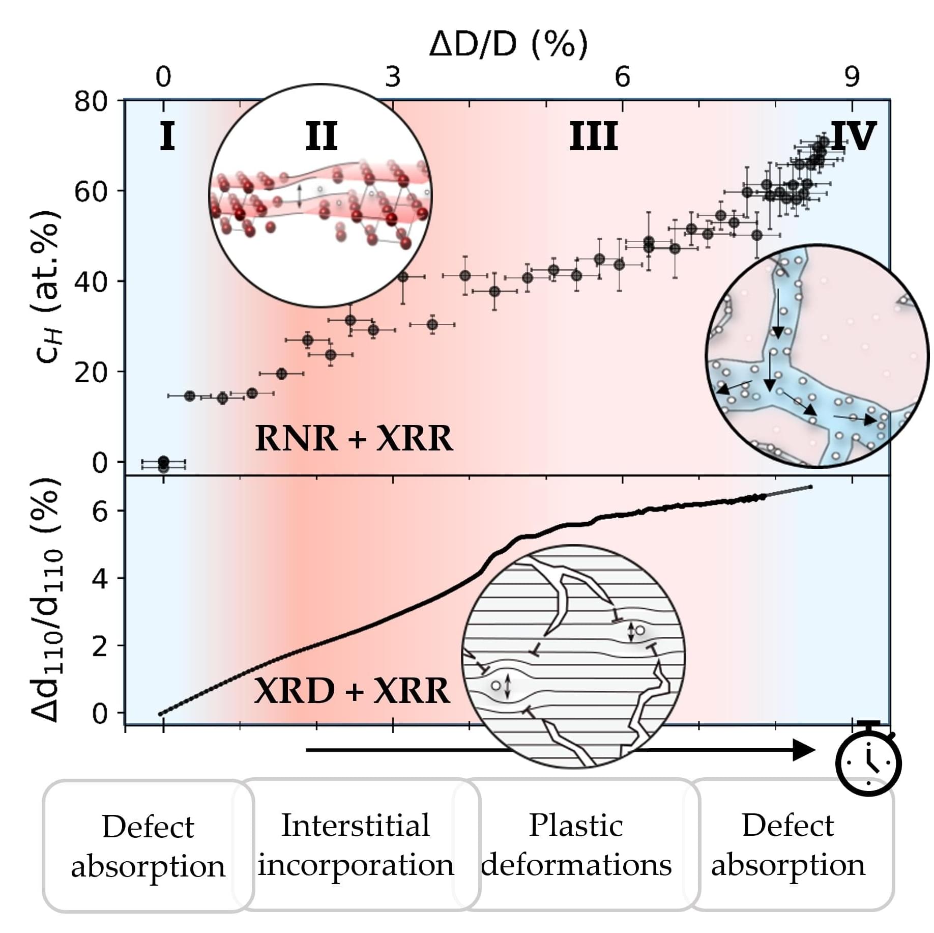
If you’re looking for hydrogen on the elemental chart, it won’t take you long to find it. It is right there at the beginning, the lightest possible material. One electron, one proton, one neutron. Simple, minimalistic, the Marie Kondo of the elemental chart, but with enormous potential in terms of possible technological applications.
A very prominent example interests every single one of us: Let’s look into the daytime sky.
If we think of the sun as a furnace, then hydrogen atoms are the coal ingots.