Experiments show signs of a material that conducts electricity in opposite directions along its edges through fractionally charged quasiparticles.
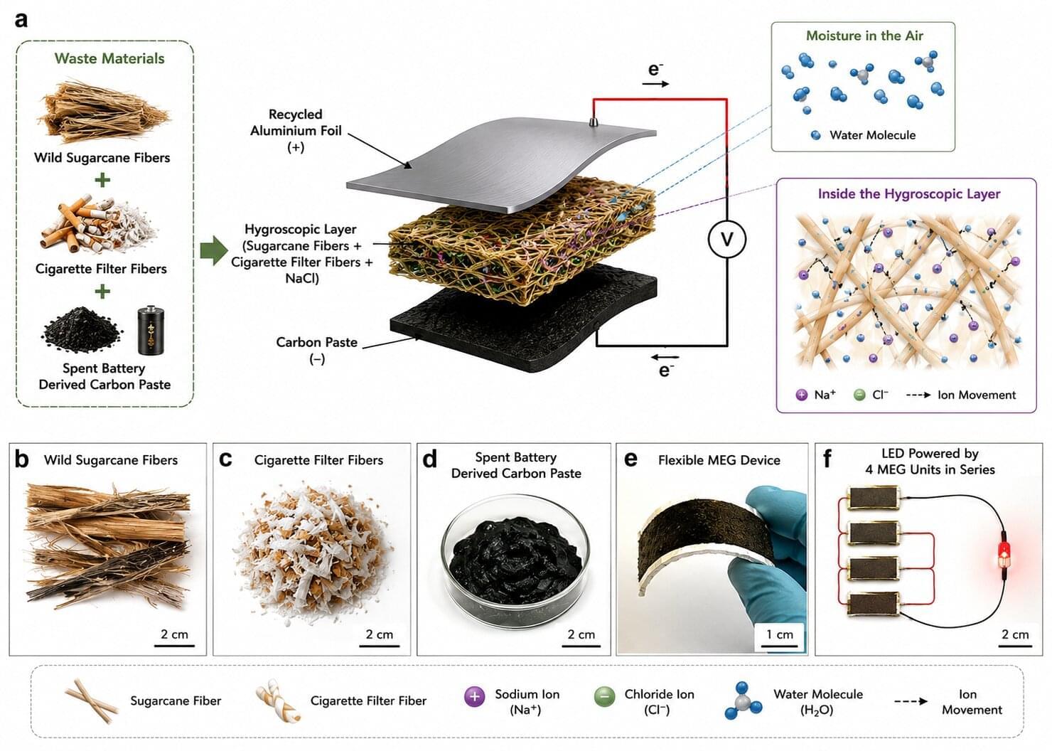
Imagine what would happen if the source of your electricity was not the sun, wind, or water flow, but rather the moisture present in the air? The ability of moisture to provide energy has been well-known for a long time, although harnessing that invisible power for generating electricity has been a difficult task. Until recently, all of the proposed generators were either inefficient or too expensive to use in real-life settings.
As reported in a study in Scientific Reports, scientists were able to create a low-cost and flexible electrical generator that harnesses the energy from moisture and also gives a second life to waste materials.
A single generator was capable of producing enough voltage (up to 1.16 volts) to surpass many of the previous humidity-based generators, and multiple generators can even provide the energy needed to light up an LED light bulb without using any external capacitors.
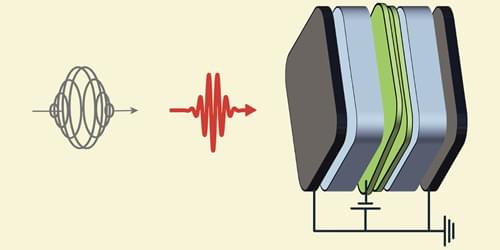
Many of the advanced electronic components surrounding us in everyday life rely on polar materials to function. Polar materials have an uneven distribution of electric charge. This gives them a positive and a negative side even in the absence of an external electric field. The most important among these are ferroelectric materials, in which the direction of polarization can be reversed by applying an electric field.
Researchers are now identifying materials that combine properties previously thought to be mutually exclusive. This could lead to new technological applications.
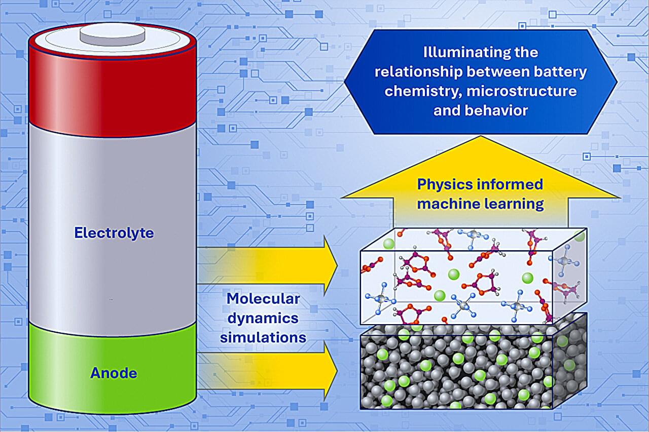
For grid-scale energy storage and national energy resilience, the U.S. needs better batteries. Lawrence Livermore National Laboratory (LLNL) scientists are tackling that challenge in many ways, but one approach is making a significant impact: physics-informed machine learning.
In two recent publications, LLNL researchers examined how integrating molecular dynamics simulations with physics-informed machine learning can illuminate the relationships between structure and behavior in complex battery materials. They used the combination of techniques to explore carbon anodes in sodium-ion batteries and liquid electrolytes in lithium-ion batteries.
“These studies show that the structural complexity of battery materials is not just an obstacle to understanding but a design advantage, laying the groundwork for high-throughput screening of next-generation energy-storage materials,” said LLNL scientist and author Liwen (Sabrina) Wan. “By encoding that complexity into physics-informed machine learning models, we can predict properties and identify design levers that traditional approaches simply cannot access.”
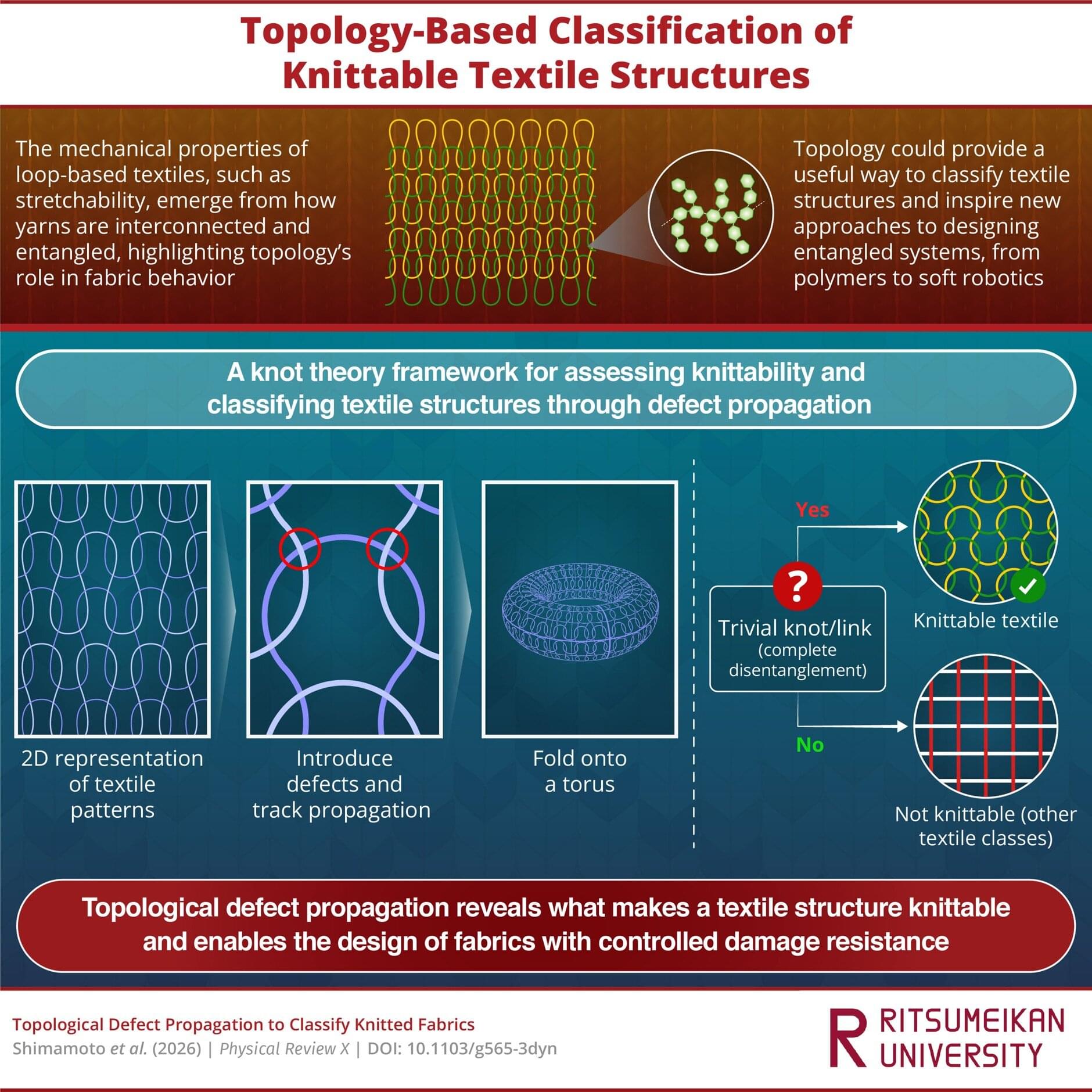
Fabrics are made by repeatedly intertwining yarns into characteristic patterns. Many of their properties, such as stretchiness, arise not only from the material itself but also from how the yarns are arranged and entangled. Such properties illustrate how topology—the underlying patterns of connectivity and entanglement within a structure—can shape a material’s overall behavior. Understanding these relationships could help researchers design materials with tailored properties through the design of their topology.
A research team led by Dr. Daisuke S. Shimamoto, a senior researcher at the Research Organization of Science and Technology, Ritsumeikan University, Japan, along with Dr. Keiko Shimamoto, an independent researcher from Tokyo, Japan, Dr. Sonia Mahmoudi from Tohoku University, and Dr. Samuel Poincloux from Aoyama Gakuin University, has developed a mathematical framework based on knot theory for characterizing knittability and classifying periodic textile structures based on how defects spread through them. Their findings were published in Physical Review X on July 14, 2026.
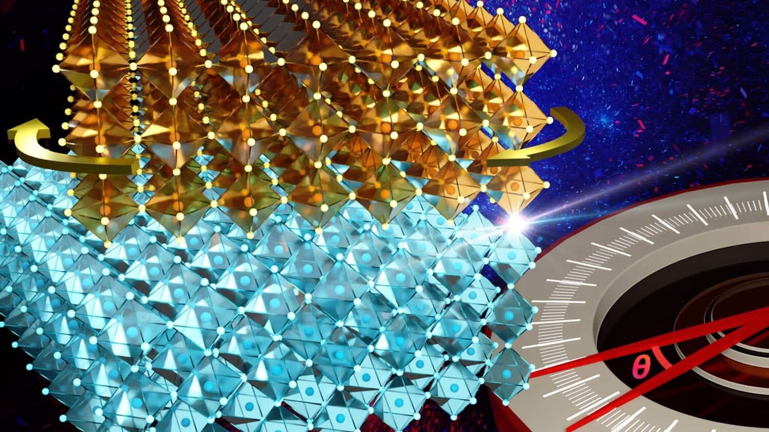
Researchers have shown it is possible to expand the field of twistronics—literally. They have demonstrated a technique that allows them to fabricate oxide twistronic materials at much larger scales while also controlling the twist angles between materials that dictate their structural and electronic properties.
The field of twistronics examines how the angle between layers of two-dimensional (2D) materials affects their electronic properties. The paper, “Deterministic Fabrication of Large-Area, High-Crystallinity Oxide Moiré Superlattices,” is published in the journal ACS Nano.
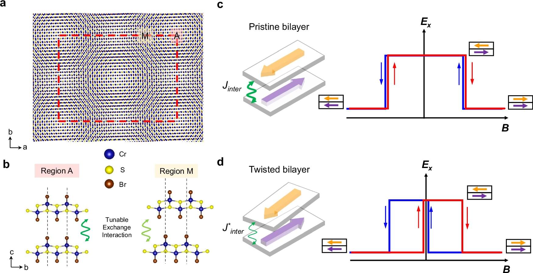
The properties of ultrathin magnets can be specifically altered by a slight twist between two atomic monolayers. This is the conclusion reached by an international research team led by TU Darmstadt in a study published in Nature Communications. The findings open new prospects for future memory devices.
For the first time, the researchers observed that an extremely thin magnetic material—a so-called two-dimensional van der Waals magnet—” stores” its magnetic state: It responds to a magnetic field and retains some of its magnetization even when the applied field changes. This “memory” is known as hysteresis and forms the basis of many data storage systems.
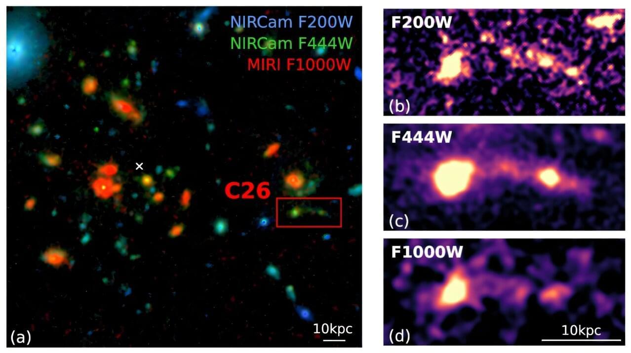
Astronomers have spotted many “red and dead” galaxies in the early universe. These are massive systems that stopped forming stars surprisingly early in cosmic history. Now, they may have found evidence of one in the act of becoming dead: a massive galaxy being stripped of its starforming gas just 1.4 billion years after the Big Bang. The clues behind why it lost its star-forming material are detailed in a paper posted to the arXiv preprint server on June 16.
Comet-like galaxy SPT2349–56 is an emerging galaxy cluster, or “protocluster,” containing about 30 star-forming galaxies within a region 100 kiloparsecs wide. Among its members, C26 is particularly interesting because of its unusual shape. It has a head and a tail like a comet. It also has a dense, bright region called the “knot,” embedded within the tail. It was first detected in ALMA images.
In this new study, using observations from the Hubble Space Telescope and the James Webb Space Telescope, the team led by Dazhi Zhou of the University of British Columbia studied this galaxy’s head, tail and knot to estimate its mass and star-forming properties.
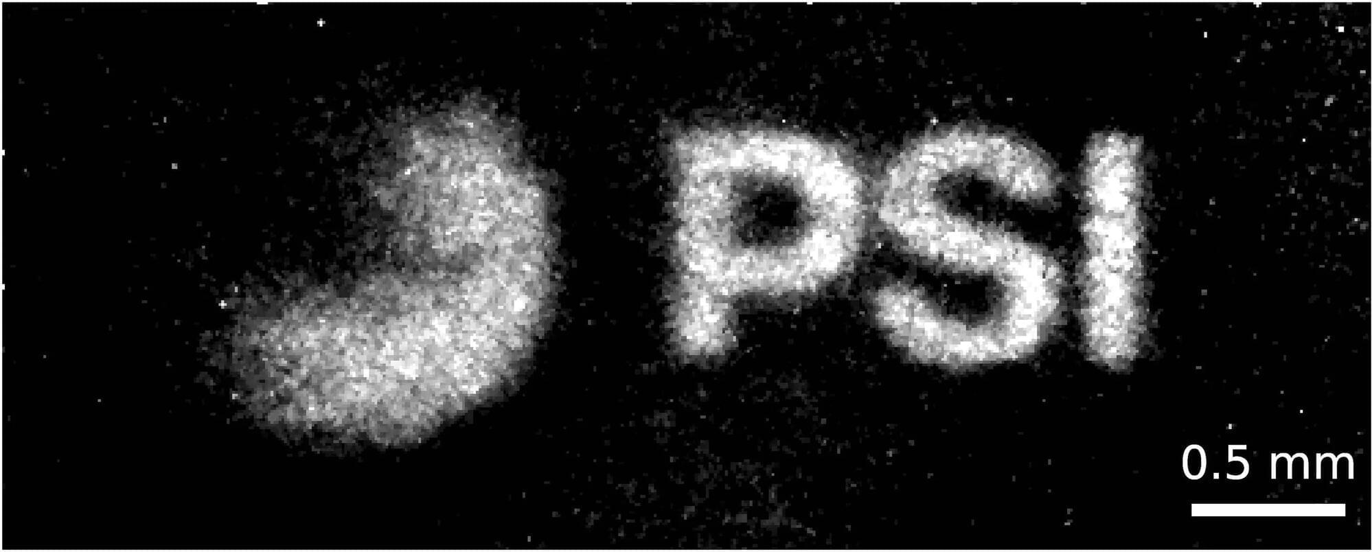
Researchers at Paul Scherrer Institute (PSI) have developed the world’s first achromatic lens for neutron imaging. The lens overcomes a longstanding obstacle in the field: focusing neutrons of different wavelengths well enough to form a sharp, magnified image. With the lens, researchers can now image thick samples and follow processes inside bulky equipment such as furnaces, cryostats or pressure cells.
Neutrons can provide unique insights into the structure of materials—but they are hard to manipulate. Neutrons, like X-rays, are produced as a beam at research facilities such as the Swiss Spallation Neutron Source SINQ and are used to image inside materials and objects. Unlike X-rays, however, neutrons can penetrate deeply into many metals while remaining highly sensitive to light elements such as hydrogen and lithium. In this way, they can be used to observe oil, polymer or lithium distribution inside dense metallic structures such as engines or batteries, reveal water uptake in plants or nondestructively examine priceless archaeological artifacts.
Yet the same weak interaction with matter that makes neutrons such a useful tool also makes them notoriously difficult to deflect or focus—a fact that has limited the development of advanced imaging techniques. Now, PSI scientists have reported in Nature Communications a new type of lens that overcomes this barrier.
When playing the classic game “20 Questions,” one may begin with the common opener: “Animal, vegetable, or mineral?”
For the ancient sea worm Perinereis cultrifera (which is still around today), the answer might not be so simple. Along with other predatory bristle worms, Perinereis cultrifera has jaws made from structural proteins and ions, which it uses for eating, crushing or biting. The unique makeup and properties of these jaws led some researchers to coin a new term to describe these types of materials: bio-metals, an emerging field of biophysical study.
The term “bio-metal” goes beyond identifiers like “metallike biomaterials” or “biomaterials with metallike properties,” which have been used in scientific literature to describe biomaterials with conductivity or strength values similar to metals. Instead, bio-metals can be categorized by three qualities: hardness, strain mechanics and ion-protein structure.