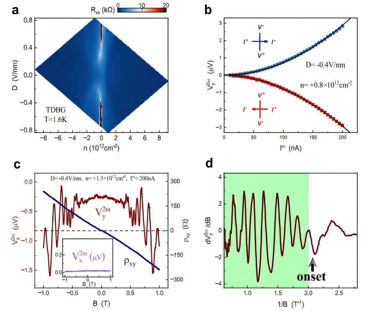
Toggle light / dark theme

Shroud of Turin image matches low-relief statue—not human body, 3D modeling study finds

The Shroud of Turin is a famous artifact with obscure origins. How and when it was made has long been the subject of debate among many scientists, historians and religious leaders, alike. The two most prominent theories are that it was either created as a work of art during the medieval period or that it was a piece of linen that was actually wrapped around the body of Jesus Christ after his death over 2000 years ago.

Radiocarbon dating done in a 1989 study on the Shroud of Turin dated it around 1,260 to 1,390 AD, consistent with the medieval theory. Later, in 2005, Raymond Rogers argued that the tested sample from the came from an area that had been repaired, and was thus newer than the original cloth. And more recently, in 2022, a single thread from the shroud material was tested with a new—and somewhat controversial—method based on Wide Angle X-ray Scattering (WAXS), which claimed that the shroud dated back to the first century AD. If those results are reliable, this dates the cloth much closer to the time of Jesus.

Yet another study examined the blood patterns on the shroud and deemed them inconsistent with what would be expected with a deceased man lying flat. In fact, the authors stated that these blood patterns were “totally unrealistic.” This led to the idea that the blood might have been added to the shroud in a more artistic manner after its creation.

First-Ever Penis and Scrotum Transplant Makes History at Johns Hopkins

Surgeons at The Johns Hopkins Hospital have performed the world’s first total penis and scrotum transplant.

The patient suffered a devastating injury several years ago from an improvised explosive device while serving in Afghanistan. He is now recovering at the hospital after the 14-hour procedure in late March, which repaired his abdominal wall, gave him a new scrotum and attached a donor penis.

“We are optimistic he will regain near-normal urinary and sexual functions,” said W. P. Andrew Lee, director of plastic and reconstructive surgery at the Johns Hopkins University School of Medicine.

A guidance to intelligent metamaterials and metamaterials intelligence

The bidirectional interactions between metamaterials and artificial intelligence have recently attracted much attention. Here, the authors stand from a unified perspective to discuss intelligent metamaterials (AI for metamaterials) and metamaterials intelligence (metamaterials for AI).

Metamaterials: Highly Twisted Rods Store Large Amounts of Energy

An international research team coordinated at KIT (Karlsruhe Institute of Technology) has developed mechanical metamaterials with a high elastic energy density. Highly twisted rods that deform helically provide these metamaterials with a high stiffness and enable them to absorb and release large amounts of elastic energy. The researchers conducted simple compression experiments to confirm the initial theoretical results. Their findings have been published in the science journal Nature. (DOI: 10.1038/s41586-025–08658-z)

Be it springs for absorbing energy, buffers for mechanical energy storage, or flexible structures in robotics or energy-efficient machines: Storage of mechanical energy is required for many technologies. Kinetic energy, i.e. motion energy or the corresponding mechanical work, is converted into elastic energy in such a way that it can be fully released again when required. The key characteristic here is enthalpy – the energy density that can be stored in and recovered from an element of the material. Peter Gumbsch, Professor for mechanics of materials at KIT’s Institute for Applied Materials (IAM), explains that achieving the highest possible enthalpy is challenging: “The difficulty is to combine conflicting properties: high stiffness, high strength and large recoverable strain.”

Clever arrangement of helically deformed rods in metamaterials.

High-quality crystals enable new insights into structure–property relationships and multifunctionality

Researchers at Kumamoto University and Nagoya University have developed a new class of two-dimensional (2D) metal-organic frameworks (MOFs) using triptycene-based molecules, marking a breakthrough in the quest to understand and enhance the physical properties of these promising materials. The work is published in the Journal of the American Chemical Society.

Molecular imaging uncovers hidden flaws in plastics used for electronics

A new study uncovers revealing insights into how plastic materials used in electronics are formed, and how hidden flaws in their structure could be limiting their performance.

Conjugated polymers are a type of plastic that conduct electricity and are used in optoelectronics, computing, biosensors, and power generation. The materials are lightweight, low-cost, and can be printed in thin layers onto flexible substrates, making them ideal for next-generation technologies.

An international team of scientists investigated a popular method for making the polymers called aldol condensation, which is praised for being versatile, metal-free, environmentally friendly, and scalable.

Northeastern discovery in quantum materials could make electronics 1,000 times faster

Researchers at Northeastern University have discovered how to change the electronic state of matter on demand, a breakthrough that could make electronics 1,000 times faster and more efficient.

By switching from insulating to conducting and vice versa, the discovery creates the potential to replace silicon components in electronics with exponentially smaller and faster quantum materials.

“Processors work in gigahertz right now,” said Alberto de la Torre, assistant professor of physics and lead author of the research. “The speed of change that this would enable would allow you to go to terahertz.”


Northeastern researchers discovered how to control quantum materials with light, potentially making electronics 1,000 times faster.

Flexible optoelectronic device with minimal defects fabricated at just 90°C

Dr. Jung-Dae Kwon’s research team at the Energy & Environmental Materials Research Division of the Korea Institute of Materials Science (KIMS) has successfully developed an amorphous silicon optoelectronic device with minimal defects, even using a low-temperature process at 90°C. The findings are published in the journal Advanced Science.

Notably, the team overcame the limitations of high-temperature processing by precisely controlling the hydrogen dilution ratio—the ratio of hydrogen to silane (SiH4) gas—enabling the fabrication of high-performance flexible optoelectronic devices (sensors that detect light and convert it into ).

Flexible optoelectronic devices are key components of next-generation , such as wearable electronics and image sensors, and require the precise deposition of thin films on thin, bendable substrates. However, a major limitation has been the necessity of high-temperature processing above 250°C, making it difficult to apply these devices to heat-sensitive flexible substrates.

Comparative Performance Analysis of Femtosecond-Laser-Written Diode-Pumped Pr: LiLuF4 Visible Waveguide Lasers

In crystalline materials, the fabrication of optical waveguides by femtosecond laser irradiation is not as easy as in glasses [7] because, in many cases, it is not possible to produce a refractive index increase, able to directly confine and guide light along a certain trajectory. On the contrary, the most typical situation is that the refractive index of the crystal is decreased by the effect of the high intensity of the laser, but even in those cases it can be used anyway to design efficient waveguides [22].

In our study, we designed and fabricated waveguides with different configurations and geometries in the search for the best performance, helping us to understand the confinement mechanisms in Pr: LLF. The following waveguide types were tested:

Researchers observe nematic order in magnetic helices, echoing liquid crystal behavior

Nematic materials are made of elongated molecules that align in a preferred direction, but, like in a fluid, are spaced out irregularly. The best-known nematic materials are liquid crystals, which are used in liquid crystal display (LCD) screens. However, nematic order has been identified in a wide range of systems, including bacterial suspensions and superconductors.

Now, a team led by researchers at the Department of Energy’s Lawrence Berkeley National Laboratory (Berkeley Lab), SLAC National Accelerator Laboratory and University of California, Santa Cruz, has discovered a nematic order in a , in which the magnetic spins of the material are arranged into coils pointing in the same general direction.

“If we think of these magnetic helices as the objects that are aligning, the magnetism follows expectations for nematic phases,” said Zoey Tumbleson, a graduate student at Berkeley Lab and the University of California, Santa Cruz, who led this work. “These phases were not previously known and it’s very exciting to see this generalized to a wider field of study.”

/* */