Toggle light / dark theme

AI model captures how humans read, paving the way to personalized text and better augmented reality

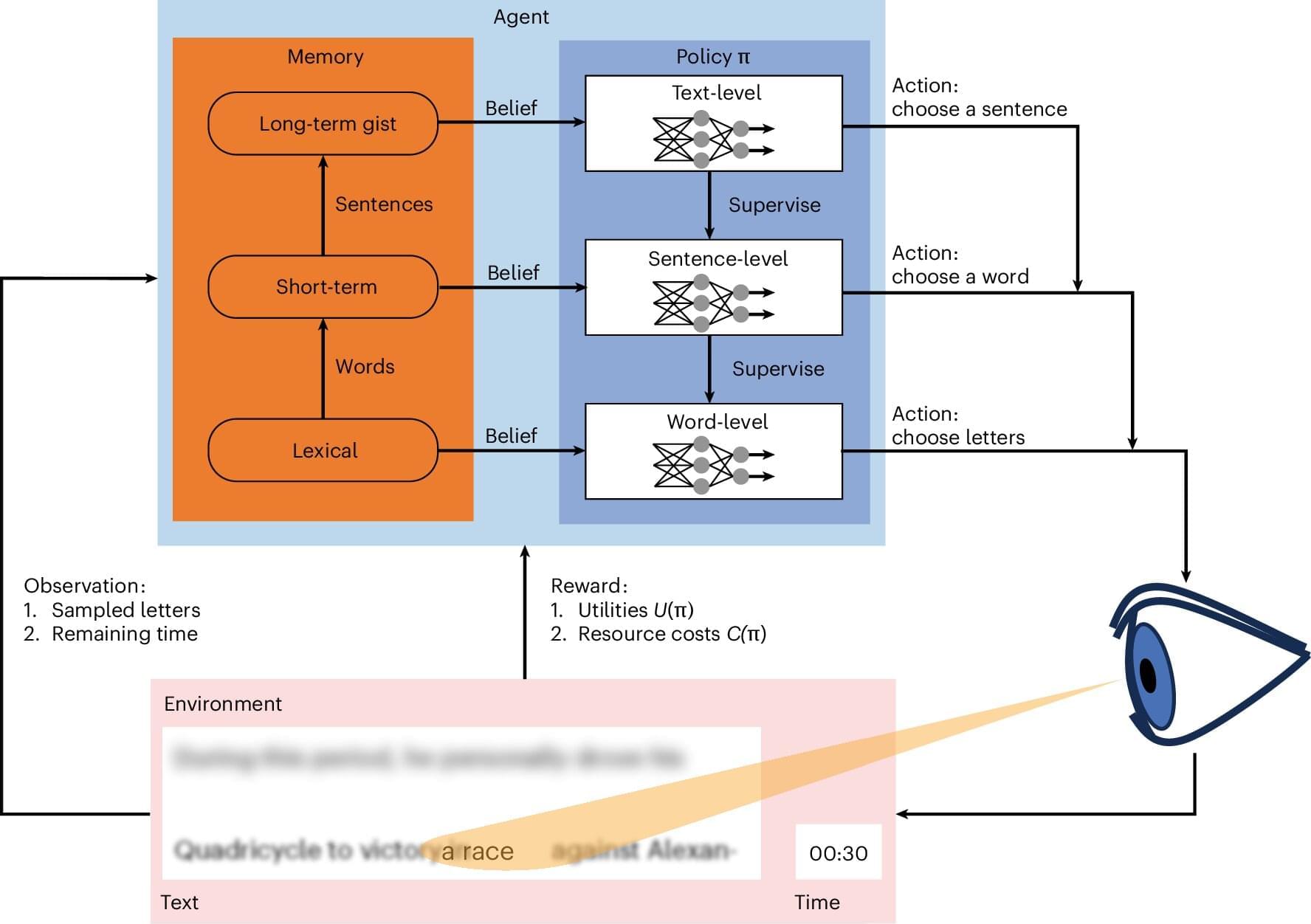
Researchers at Aalto University, together with international partners, have developed the most accurate model yet of how humans read. The new model uses reinforcement learning, a type of AI used in robotics, to explain—and recreate—the choices readers make as they move through text.

“For the first time we’ve used AI methods to understand—not just mimic—how people read,” says Professor Antti Oulasvirta from Aalto University. In a study to be published Monday, Aug. 10, in Nature Human Behaviour, researchers say the model could power smarter augmented reality (AR) displays and tailor complex texts to different readers and everyday situations.

Earlier models learned from large data sets pairing text snippets with eye-tracking data, then mimicked human behavior, but they lacked true understanding of the content and didn’t generalize well across languages or contexts, Oulasvirta explains. In contrast, the new model follows the psychological mechanisms readers use to direct attention, revealing how understanding is built as the eyes move through words, sentences and paragraphs.
Holographic Breakthrough: This New Futuristic 3D Imaging System Overcomes a Longstanding Problem for Holographic Tech

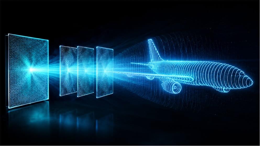
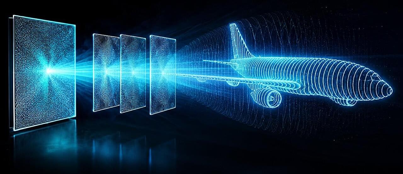
A new 3D image projection system from researchers at the UCLA Samueli School of Engineering and the California NanoSystems Institute (CNSI) marks a major step toward overcoming a longstanding problem for holographic technology.

Professor Aydogan Ozcan led the work reported in a recent paper published in Light Science and Applications, which describes the team’s new snapshot 3D image projection system, solving one of the technology’s most daunting issues.

“These results establish the diffractive 3D display system as a compact and scalable framework for depth-resolved snapshot 3D image projection, with potential applications in holographic displays, AR/VR interfaces, and volumetric optical computing,” the authors write.

Light-programmed system projects 28-layer 3D images in single shot

Researchers at the UCLA Samueli School of Engineering and CNSI (California NanoSystems Institute), led by Professor Aydogan Ozcan, introduced a snapshot 3D image projection system that integrates a digital encoder with a passive diffractive optical decoder, jointly optimized end-to-end through deep learning. The hybrid architecture projects multiple distinct images onto closely spaced axial planes in a single shot, marking a significant step toward compact, high-fidelity volumetric display technologies. The research is published in the journal Light: Science & Applications.

3D image display technology is essential for next-generation holography, immersive visualization, and augmented and virtual reality (AR/VR) interfaces, where accurate focal cues across depth are critical for natural depth perception and visual comfort. However, dense depth multiplexing in conventional holographic displays remains a challenge: As the axial image planes approach one another in the output volume, diffraction-induced crosstalk rapidly degrades depth selectivity and image fidelity.

Transparent OLED advance could improve AR displays and smart windows

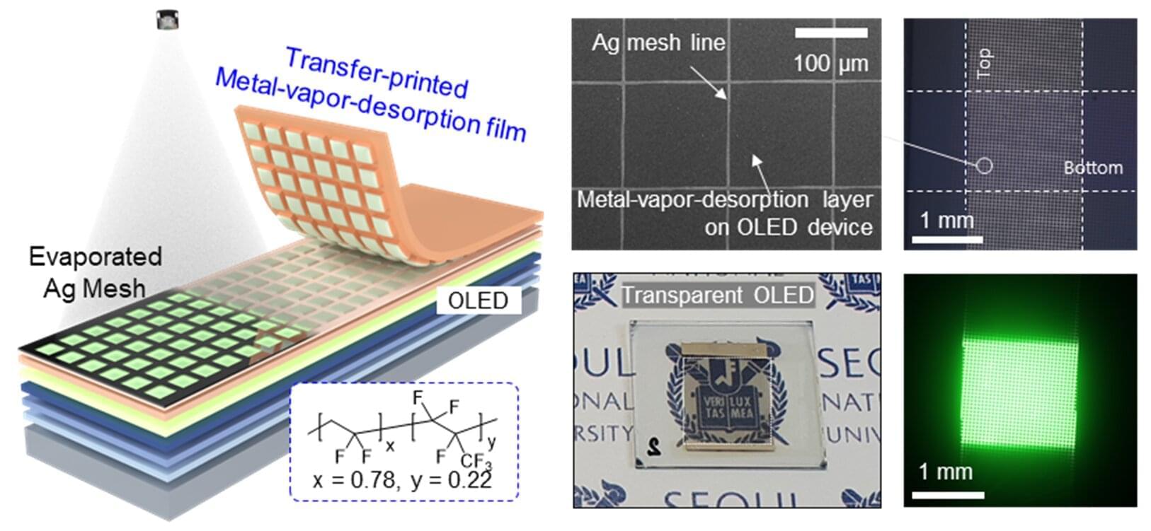
Seoul National University College of Engineering announced that a research team led by Prof. Yongtaek Hong from the Department of Electrical and Computer Engineering has developed a high-performance transparent organic light-emitting diode (OLED) incorporating highly conductive transparent metal mesh top electrodes fabricated using a selective metal deposition technique. The research was published in the journal Materials Horizons and was selected as the outside front cover image for the issue.

Transparent OLEDs have attracted significant attention for next-generation applications, including advanced displays, augmented reality (AR), automotive displays and smart windows, because of their capability for bidirectional light emission. However, despite achieving high optical transparency and excellent electrical performance, conventional transparent electrodes often face limitations when directly integrated into OLED devices because their fabrication processes can chemically or physically damage the underlying organic layers.

To address this challenge, the research team developed a metal-patterning technology based on a high-resolution transfer-printing process using a metal-vapor-desorption layer (MVDL). This approach enables the fabrication of highly conductive transparent metal mesh patterns with micrometer-scale resolution without requiring chemical washing or lift-off processes. As a result, high-quality vapor-deposited metal patterns can be directly formed on organic stacks while minimizing damage to the underlying organic device layers.

Teaching AI to design optical surfaces using real-world imperfections

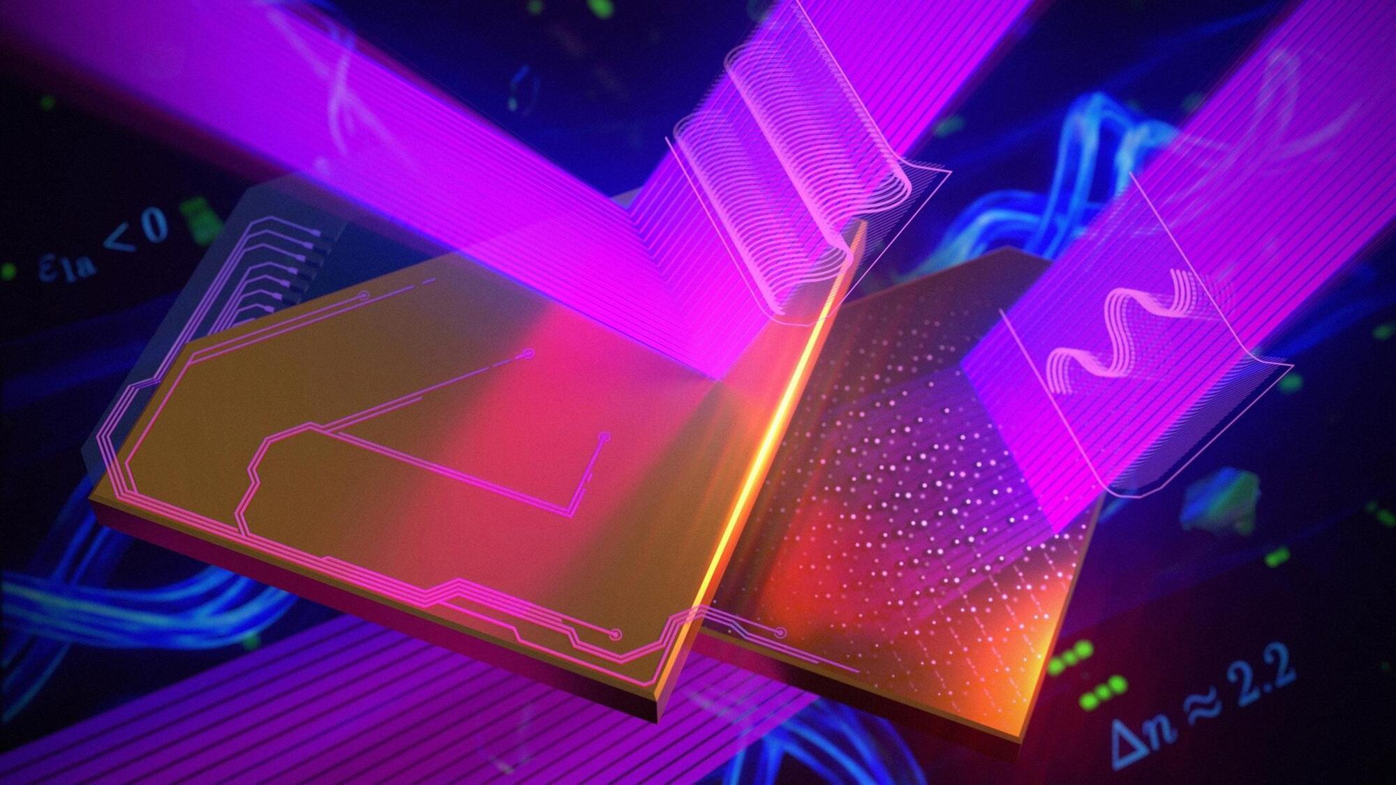
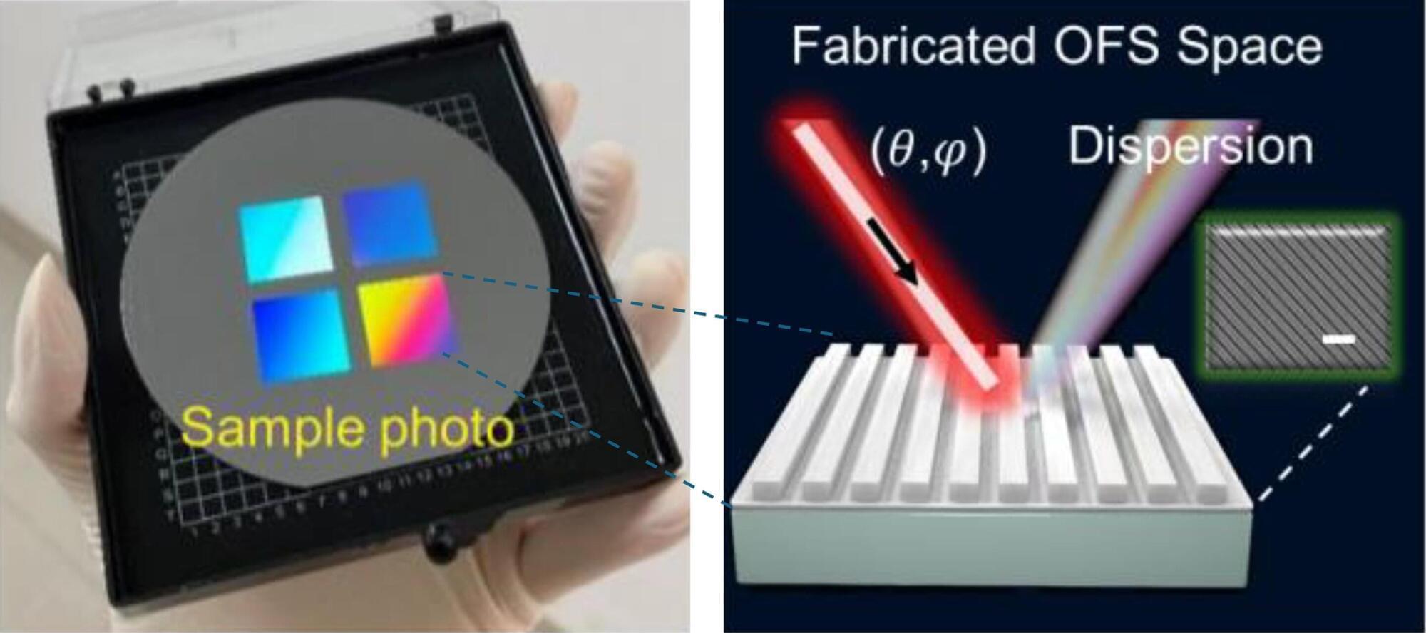
Designing surfaces that precisely control how light behaves at the nanoscale is tricky. Optical Fourier surfaces, which are nanostructured gratings that redistribute light into specific directions and wavelengths, hold enormous potential for compact spectrometers, augmented-reality displays, and advanced sensors. However, their standard design process relies on computer simulations that assume idealized conditions such as single-angle illumination and the absence of fabrication imperfections—a far cry from reality.

The gap between what simulations predict and what fabricated devices actually do has long frustrated researchers. It widens further when designers try to exploit one of the most powerful but underused design parameters: the angle of incoming light. Changing the incident angle can activate or suppress optical modes without any physical modification to the structure, effectively enabling multiple functions on a single device.

“This effectively introduces an additional degree of freedom beyond geometry, expanding the design space significantly,” said Associate Professor Dong Zhaogang from the Singapore University of Technology and Design (SUTD). “But its practical use has been limited because simulations at oblique incidence are often computationally unstable and costly, while real experimental systems involve angular distributions rather than single-incident angles.”

Smartphones may soon be able to track hidden objects using LiDAR

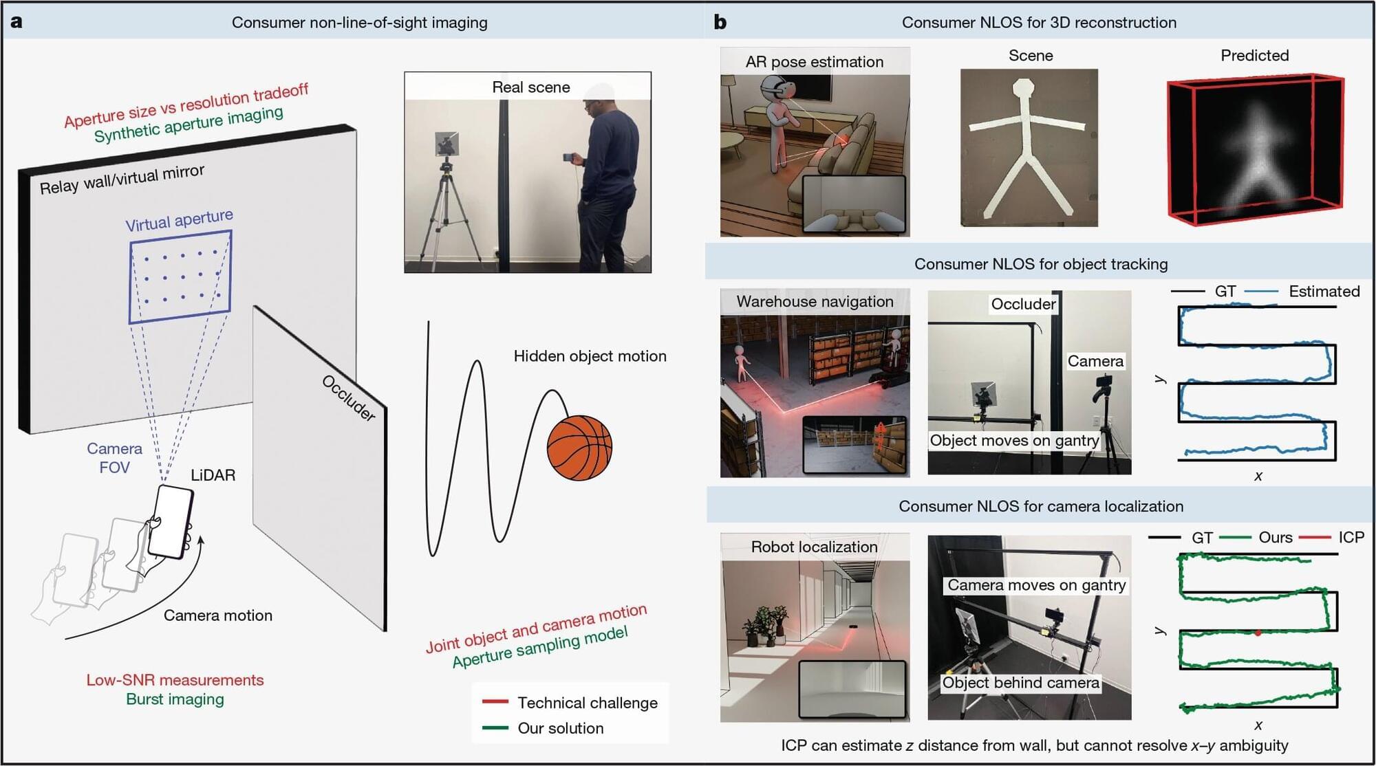
Modern smartphones are packed with incredible technology, from high-resolution cameras and advanced graphics chips to AI processors. In premium models, this hardware includes LiDAR (light detection and ranging), which helps power augmented reality features and improve depth sensing.

And that capability could soon be in for a seriously impressive upgrade. Researchers at the Massachusetts Institute of Technology (MIT) have developed an algorithm that lets a phone’s LiDAR sensor detect objects hidden around corners. Details are in a paper published in the journal Nature.

Typically, this type of non-line-of-sight (NLOS) capability is found in labs and relies on bulky, expensive research-grade hardware. But the team’s breakthrough makes it possible for consumer LiDAR sensors to peek behind obstacles.

Hybrid projector delivers super-resolution images across extended depth with 16-fold gain

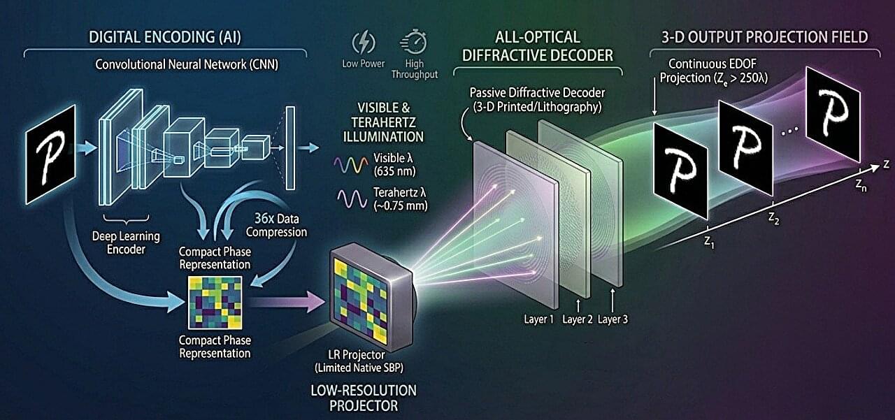
Researchers at the University of California, Los Angeles (UCLA) have developed a novel image projection system that delivers super-resolution images over an extended depth of field. By combining a neural network-based digital encoder with a passive all-optical diffractive decoder, the system drastically compresses image data for efficient transmission of image information. This platform operates without extra power at the decoding stage, promising advancements for next-generation virtual and augmented reality displays.

The study is published in the journal Light: Science & Applications.

A research team led by Professors Aydogan Ozcan and Mona Jarrahi, along with UCLA graduate student Hanlong Chen, designed a system that divides the image projection workload into two parts.

/* */