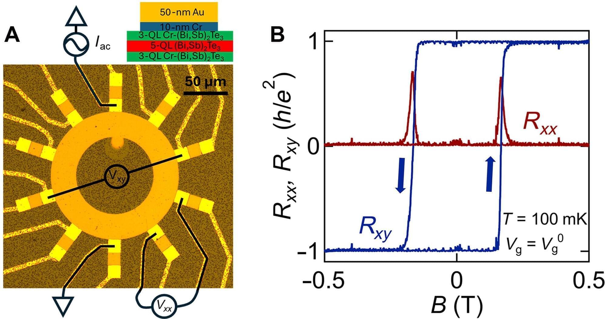
Toggle light / dark theme

String Theory Inspires a Brilliant, Baffling New Math Proof

When the team posted their proof in August, many mathematicians were excited. It was the biggest advance in the classification project in decades, and hinted at a new way to tackle the classification of polynomial equations well beyond four-folds.

But other mathematicians weren’t so sure. Six years had passed since the lecture in Moscow. Had Kontsevich finally made good on his promise, or were there still details to fill in?

And how could they assuage their doubts, when the proof’s techniques were so completely foreign — the stuff of string theory, not polynomial classification? “They say, ‘This is black magic, what is this machinery?’” Kontsevich said.

Time might not exist — and we’re starting to understand why

Consider two events, A and B, such as flashes of light made by two sources in different places.

Cause and effect means there are three possibilities: 1) Flash A happened before flash B, and via some mechanism, could have triggered B; 2) Flash B happened before Flash A and could have triggered it; 3) Neither one could have triggered the other because they are too far apart in space and too close in time for a triggering signal to have been sent from one location to the other.

Now, Einstein’s Special Theory of Relativity states that all observers, no matter how fast they’re moving relative to each other, see light travelling at the same constant speed.

This strange but simple fact can lead to observers seeing events happening in different orders.

For option above, two observers moving relative to each other close to the speed of light might disagree on the ordering of flashes.

Thankfully, there’s no danger of an effect coming before its cause (known as a ‘violation of causality’) since the events are too far apart for either to cause the other.

However, what if options and coexisted in a quantum superposition? The causal order of the two events would no longer be fixed.

From fullerenes to 2D structures: A unified design principle for boron nanostructures

Boron, a chemical element next to carbon in the periodic table, is known for its unique ability to form complex bond networks. Unlike carbon, which typically bonds with two or three neighboring atoms, boron can share electrons among several atoms. This leads to a wide variety of nanostructures. These include boron fullerenes, which are hollow, cage-like molecules, and borophenes, ultra-thin metallic sheets of boron atoms arranged in triangular and hexagonal patterns.

Dr. Nevill Gonzalez Szwacki has developed a model explaining the variety of boron nanostructures. The analysis, published in the journal 2D Materials, combines more than a dozen known boron nanostructures, including the experimentally observed B₄₀ and B₈₀ fullerenes.

Using first-principles quantum-mechanical calculations, the study shows that the structural, energetic, and electronic properties of these systems can be predicted by looking at the proportions of atoms with four, five, or six bonds. The results reveal clear links between finite and extended boron structures. The B₄₀ cage corresponds to the χ₃ borophene layer, while B₆₅, B₈₀, and B₉₂ connect with the β₁₂, α, and bt borophene sheets, respectively. These structural links suggest that new boron cages could be created by using known two-dimensional boron templates.

Growth strategy enables coherent quantum transport in single-layer MoS₂ semiconductors

Two-dimensional (2D) semiconductors are thin materials (i.e., one-atom thick) with advantageous electronic properties. These materials have proved to be promising for the development of thinner, highly performing electronics, such as fitness trackers and portable devices.

A 2D semiconductor that has attracted particular interest within the electronics community is molybdenum disulfide (MoS₂), a transition-metal dichalcogenide made up of one metal atom and two chalcogen atoms. To build reliable large-area electronics based on MoS₂ layers, engineers need to uniformly grow this material over wafer-scale surfaces, minimizing defects that hinder the performance of devices.

Researchers at the Institute for Basic Science (IBS), Pohang University of Science and Technology (POSTECH) and other institutes recently introduced a new approach to grow single-layer MoS₂ on substrates while maintaining a uniform atomic arrangement. Their approach, outlined in a paper in Nature Electronics, entails a greater control of the process by which small crystal regions merge on a substrate, also known as coalescence.

Real-life ‘quantum molycircuits’ using exotic nanotubes

Molybdenum disulfide MoS2 is a groundbreaking material for electronics applications. As a two-dimensional layer similar to graphene, it is an excellent semiconductor, and can even become intrinsically superconducting under the right conditions. It’s not particularly surprising that science fiction authors have already been speculating about molycircs, fictional computer circuits built from MoS2, for years—and that physicists and engineers are directing huge research efforts at this material.

Researchers at the University of Regensburg, have many years of expertise with diverse quantum materials—in particular also with carbon nanotubes, tube-like macromolecules made from carbon atoms alone.

“It was an obvious next step to now focus on MoS2 and its fascinating properties,” said Dr. Andreas K. Hüttel, head of the research group Nanotube Electronics and Nanomechanics in Regensburg. In cooperation with Prof. Dr. Maja Remškar, Jožef Stefan Institut Ljubljana, a specialist in the crystalline growth of nanomaterials, his research group started working on based on MoS2 nanotubes.

All-optical modulation in silicon achieved via an electron avalanche process

Over the past decades, engineers have introduced numerous technologies that rely on light and its underlying characteristics. These include photonic and quantum systems that could advance imaging, communication and information processing.

A key challenge that has so far limited the performance of these new technologies is that most materials used to fabricate them have a weak optical nonlinearity. This essentially means that they do not strongly change in response to light of different intensities.

A strong optical linearity is of crucial importance for the development of ultrafast optical switches, devices that can control either light or electrical signals by modulating the properties of a light-based signal (e.g. its intensity or path). Notably, these switches are central components of fiber optics-based communication systems, photonic devices and quantum technologies.

Colloidal quantum dot photodiodes integrated on metasurfaces for compact SWIR sensors

This week, at the IEEE International Electron Devices Meeting (IEDM 2025), imec, a research and innovation hub in advanced semiconductor technologies, successfully demonstrated the integration of colloidal quantum dot photodiodes (QDPDs) on metasurfaces developed on its 300 mm CMOS pilot line. This pioneering approach enables a scalable platform for the development of compact, miniaturized shortwave infrared (SWIR) spectral sensors, setting a new standard for cost-effective and high-resolution spectral imaging solutions.

Short-wave infrared (SWIR) sensors offer unique capabilities. By detecting wavelengths beyond the visible spectrum, they can reveal contrasts and features invisible to the human eye and can therefore see through certain materials such as plastics or fabrics, or challenging conditions like haze and smoke. Conventional SWIR sensors remain, however, expensive, bulky, and challenging to manufacture, restricting their use to niche applications.

Quantum dot (QD) image sensors, a new class of SWIR sensors, offer a promising alternative, combining lower cost with higher resolution. So far, however, they have operated in broadband rather than in spectral mode.

Tiny optical modulator could enable giant future quantum computers

Researchers have made a major advance in quantum computing with a new device that is nearly 100 times smaller than the diameter of a human hair.

Published in the journal Nature Communications, the breakthrough optical phase modulators could help unlock much larger quantum computers by enabling efficient control of lasers required to operate thousands or even millions of qubits—the basic units of quantum information.

Critically, the team of scientists have developed these devices using scalable manufacturing, avoiding complex, custom builds in favor of those used to make the same technology behind processors already found in computers, phones, vehicles, home appliances—virtually everything powered by electricity (even toasters).

/* */