Toggle light / dark theme

Immune cells get transformed into fungus-fighting nanoparticles

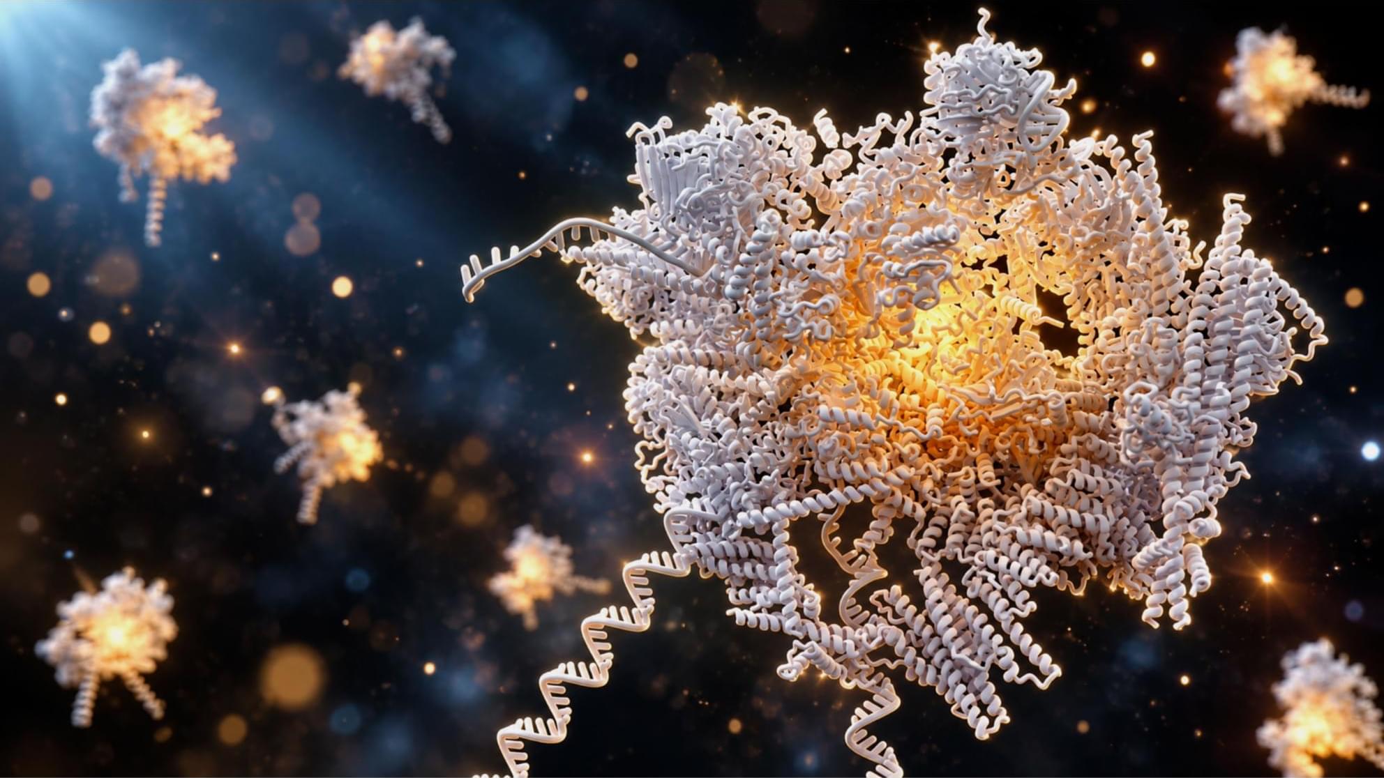
Tiny particles made from the membranes of human immune cells could offer a promising new way to fight fungal infections that are becoming harder to treat. Engineers at the University of California San Diego created antifungal nanoparticles that target Candida albicans, a fungus responsible for oral and vaginal yeast infections as well as life-threatening bloodstream infections. In mice with severe Candida infections, the nanoparticles greatly reduced the amount of fungus in major organs and significantly improved survival.

The research, published in Cell Biomaterials, was led by Liangfang Zhang, a professor in the Aiiso Yufeng Li Family Department of Chemical and Nano Engineering at the UC San Diego Jacobs School of Engineering, who also holds the Joan and Irwin Jacobs Chancellor’s Endowed Chair in Innovations for Engineering in Medicine.

DNA origami turns secret messages into nano–Morse code that acts as multiplayer molecular encryption

Mathematics has always been at the core of securing information. From online banking to government communications, modern society relies on cryptography, in which complex mathematical algorithms transform readable information into an unreadable form to keep it secure. But as computing power grows and quantum technology advances, these mathematical safeguards are increasingly vulnerable to being broken. That’s where biology stepped in.

Choosing DNA as their information protector, researchers from China developed a multilayer encryption device that takes advantage of the double-helix molecule’s programmable nature to create an origami structure that can store information with high security.

This new system used tiny, custom-built rectangular structures made of DNA, in which researchers stored the message as dots and dashes, creating a nanoscale version of Morse code. To hide the message further, they turned the flat DNA origami surfaces into tubes, physically blocking the patterns from being read or imaged. With the help of a matching unlocking key, the recipient can trigger a reaction that unrolls the DNA back to its flat form, allowing them to read and verify the message.

Computer-guided electricity rapidly transforms flat nanofilms into 3D shapes on demand

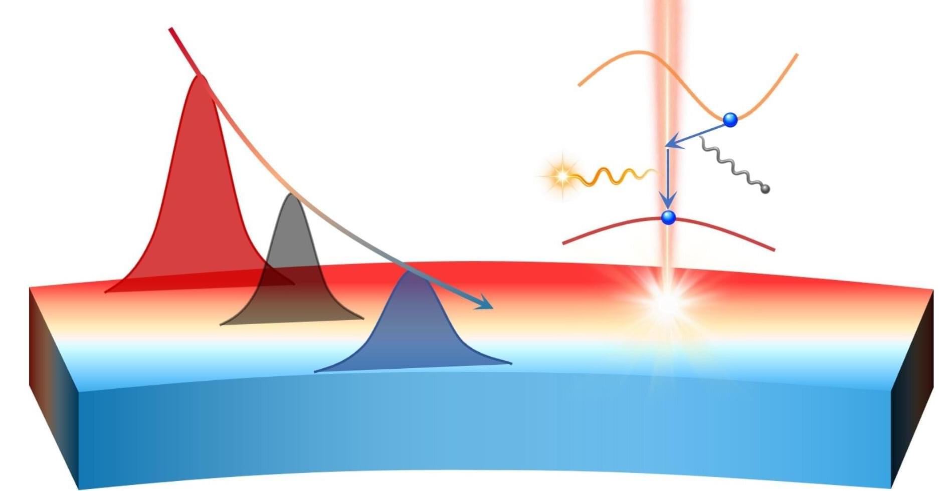
Researchers at Nagoya University in Japan have developed a method to form dome-shaped bumps on nanofilms in water using a computer-guided electron beam. The bumps form within 10 seconds and can be flattened, reshaped or repositioned as needed.

This method may enable computer-guided manipulation of nanomachines for uses such as microscale touch sensing, guiding cellular growth and direct assembly of colloidal particles. The findings were published in the journal ACS Applied Materials & Interfaces.

Existing approaches each have drawbacks: Light-based techniques typically take 60 seconds or more per shape change, while electrical methods rely on fixed electrodes that restrict where reshaping can occur and limit the size of the change.

Reimagining the furnace: How a new magnetic design could supercharge industrial plasma

Imagine trying to trap a miniature star inside a machine without letting it touch the walls or burn itself out. This is the central, high-stakes challenge of high-temperature plasma engineering.

High-temperature plasma systems are crucial for modern industry. They serve as the foundation for manufacturing semiconductors, synthesizing advanced nanomaterials and testing materials meant for extreme environments. However, for decades, these systems have been held back by three major engineering bottlenecks: low energy-conversion efficiency, chaotic plasma instability and rapid material degradation caused by punishing heat.

In my recent paper published in IEEE Transactions on Plasma Science, I set out to tackle these limitations by designing a completely new type of non-nuclear reactor: the Spherical Magnetically Stabilized Plasma Furnace, or SMSPF. My initial goal was to step away from traditional linear or cylindrical reactor designs to see whether a spherical geometry could inherently solve containment issues.

The Future Will Be Shaped By Accelerated Technological Development And Visionary Leadership

Chuck Brooks is the president of Brooks Consulting International and one of Executive Mosaic’s GovCon Experts.

We are on the brink of a transformative era where rising technologies are colliding to create unparalleled innovation. artificial intelligence, nanotechnology and quantum technologies are transforming research and development, expediting prototyping and disrupting various industries.

This convergence, propelled by exponential processing power, molecular precision and intelligent systems, promises trillions in economic value while posing significant concerns in security, ethics and labor preparedness.

New method brings single-particle quality control to nanocrystal manufacturing

Nanocrystals are already used in millions of devices, including televisions, laptops and displays, and are considered key materials for the next generation of quantum, sensing and solar technologies. However, they have not yet fully realized their potential. One major reason is their inherent heterogeneity: A single solution contains billions of nanocrystals whose properties can differ substantially. Although these particles can be characterized, important quality parameters are typically accessible only as average values across the entire sample.

“For their function in devices, these average values are insufficient,” says Professor Emiliano Cortés, who conducts research at LMU’s Nano-Institute. “Each individual nanoparticle can behave differently—for example, in its size or in how efficiently it emits light, meaning how effectively it converts absorbed energy back into light.”

China supercharges AI with 100-fold faster optical chip breakthrough

A PERSONAL SUPER COMPUTER “MACRO-CHIP” WITH PHOTONIC INTERCONNECTS:

This will soon become possible by the cheap nano-imprinting of hundreds of smaller microchips, without the need for laser lithography, onto a single monolithic wafer, with these chips’ communicating with each other at light speed as a single system via silicon photonics. A team at Peking University has set this race in motion in a major way by developing an optical system to boost AI speeds 100-fold by optical interconnects between individual microchips. The next step will be placing all of those chips onto a single monolithic wafer with a similar communication system between them. Nano-imprinting at large node-scale of 15 or 20 nm will make it possible to mass produce wafer scale systems that combine all the best types of computing features, from logic gates to optical AI accelerators in one compact package on a single wafer. Consumers will not care if the computer chips in their computers are not 14-mm wide 2-nm node chips printed by expensive extreme ultraviolet lithography, but are, instead, 8-inch or 12-inch wide super computer “macro-chips” that give 1,000 times the computing power and speed of the best Nvidia computer on the market today, whereon the distance of the individual chiplets on the wafer from the central optical multiplexer becomes part of the ingrained clock feature of the chip, replacing the traditional clock-time limit. The mother boards, GPUs and CPUs of these systems will all exist on the same wafer and communicate at light speed, with the equivalent of something like 1,000 VRAM of unified memory.

These developments come as the shrinking of traditional silicon microchips is facing a final limit. In the same way that the Personal Computer became the game-changer in the 1980’s, it appears that Personal Super-Computers will become the new kid on the block in the 2030’s.


Peking University researchers develop new all-optical interconnect system linking standard electronic chips with specific algorithms.

Researchers find simple solution for extending the lifespan of LEDs made from glowing quantum dots

A new study led by MIT researchers could drive the development of more energy-efficient digital displays—such as flat-screen TVs, augmented and virtual reality headsets, smartphone screens, medical imaging devices and even large-area ambient lighting surfaces—that also generate richer, brighter colors.

The MIT scientists, in collaboration with researchers at Samsung, studied the microscopic changes that occur inside LEDs that use electrically excited quantum dots, which are precisely shaped nanoscale semiconductor particles that emit extremely pure colored light. The research appears in Science Advances.

Quantum dots are currently used in some of the computer and television displays with the best picture quality available. The efficiency of these displays could be further improved, and their manufacturing process further simplified, if the quantum dots could be electrically excited, as was first demonstrated in the quantum dot LED (QD-LED) structures more than 20 years ago.

Common nanostructures may explain shared photoproperties in two widespread dark materials

A newly developed framework for understanding the photoproperties of both natural organic matter and eumelanin, a natural pigment responsible for dark colors in organisms, may inspire advanced sustainable technologies, scientists say.

Although they are some of the most widespread substances on Earth, not much is known about eumelanin or natural organic matter (NOM)—a dark-colored substance formed by the decomposition of biological material. In humans, eumelanin is a vital pigment in skin and other tissues that protects cells from damage caused by ultraviolet radiation. In nature, NOM gives rivers and soils their color and affects light-driven reactions like photosynthesis.

Although these compounds have been studied individually for decades, researchers in a new study, by scrutinizing them alongside each other, have shown that eumelanin and NOM have common properties beyond their dark colors.

/* */