*This video was recorded at ‘Paths to Progress’ at LabWeek hosted by Protocol Labs & Foresight Institute.*
Protocol Labs and Foresight Institute are excited to invite you to apply to a 5-day mini workshop series to celebrate LabWeek, PL’s decentralized conference to further public goods. The theme of the series, Paths to Progress, is aimed at (re)-igniting long overdue progress in longevity bio, molecular nanotechnology, neurotechnology, crypto & AI, and space through emerging decentralized, open, and technology-enabled funding mechanisms.
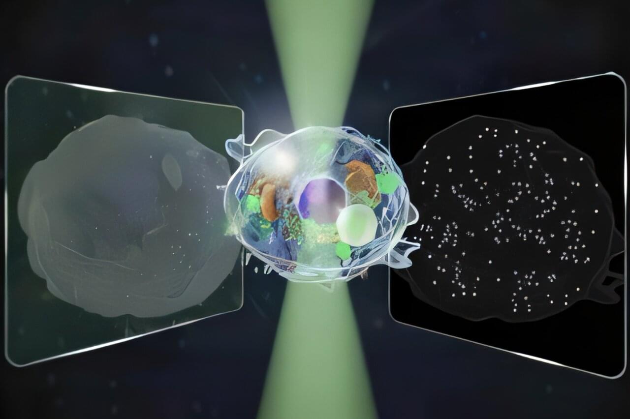
*This mini-workshop is focused on Paths to Progress in Molecular Nanotechnology*
Molecular manufacturing, in its most ambitious incarnation, would use programmable tools to bring together molecules to make precisely bonded components in order to build larger structures from the ground up. This would enable general-purpose manufacturing of new materials and machines, at a fraction of current waste and price. We are currently nowhere near this ambitious goal. However, recent progress in sub-fields such as DNA nanotechnology, protein-engineering, STM, and AFM provide possible building blocks for the construction of a v1 of molecular manufacturing; the molecular 3D printer. Let’s explore the state of the art and what type of innovation mechanisms could bridge the valley of death: how might we update the original Nanotech roadmap; is a tech tree enough? how might we fund the highly interdisciplinary progress needed to succeed: FRO vs. DAO?
*About The Foresight Institute*
The Foresight Institute is a research organization and non-profit that supports the beneficial development of high-impact technologies. Since our founding in 1986 on a vision of guiding powerful technologies, we have continued to evolve into a many-armed organization that focuses on several fields of science and technology that are too ambitious for legacy institutions to support. From molecular nanotechnology, to brain-computer interfaces, space exploration, cryptocommerce, and AI, Foresight gathers leading minds to advance research and accelerate progress toward flourishing futures.
*We are entirely funded by your donations. If you enjoy what we do please consider donating through our donation page:* https://foresight.org/donate/
