Toggle light / dark theme

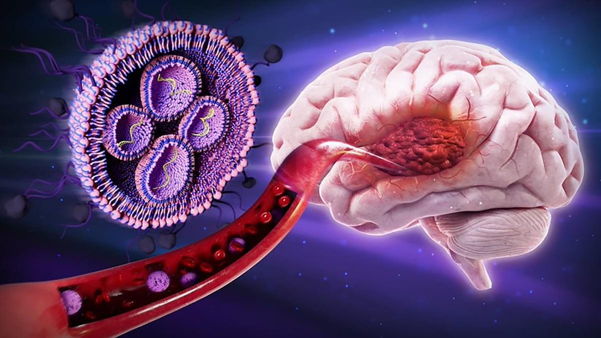
Parkinson’s-linked α-synuclein blocks protein transport in neurons, disrupting cells’ waste recycling

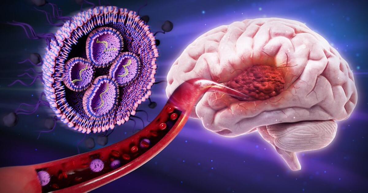
Parkinson’s disease affects more than 10 million people worldwide. The disease is characterized by the buildup of abnormal clumps of the protein alpha-synuclein inside brain cells, but scientists have long struggled to understand exactly how these toxic forms of the protein cause neurons to malfunction and eventually die.

Researchers from the Tofaris lab, part of the Nuffield Department of Clinical Neurosciences and based in the Kavli Institute for Nanoscience Discovery, combined advanced molecular analyses of human stem cell models of Parkinson’s disease with studies of postmortem brain tissue from people with Parkinson’s disease to investigate the earliest stages of the disease process.

The study is published in the journal Nature Communications.

Never-before-seen woven structure that forms naturally inside a crystal discovered

For the first time, scientists have observed a three-dimensional woven structure forming naturally inside a crystal, revealing a previously unknown way in which matter can organize itself.

Published in Light: Science & Applications, the study reports the observation of a three-dimensional woven fabric of interlaced nano-dipole ensembles that emerges spontaneously in a ferroelectric crystal as it cools through its phase transition. Unlike conventional ferroelectric crystals, in which ferroelectric domains consist of aligned electric dipoles, the dipoles in this material spontaneously weave over and under one another, creating an intricate three-dimensional network that resembles woven fabric—a type of organization never before observed in a solid crystal.

The researchers also found that they could change small parts of the woven network using a tightly focused green laser. The light locally untangles the woven pattern without affecting the rest of the crystal. Heating the crystal and cooling it again restores the woven structure, but with a new pattern.

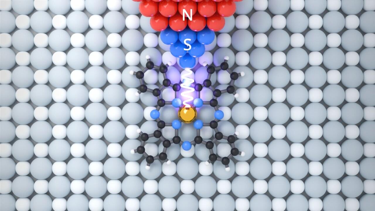
Electrostatic nanocorral offers new control over charged excitons and quantum light

Researchers created an electrically tunable quantum nanoscale corral that traps charged excitons and enables precise electrical control of tiny light sources, including their brightness, color and quantum states, the team, led by Boston College physicists, reports today in Nature Nanotechnology.

The findings open new ways to control hybrid charge, photon and spin quantum states.

Nano-optics: New mechanism for channeling light waves discovered in natural hyperbolic materials

Researchers at the 4th Physics Institute of the University of Stuttgart and the Istituto Italiano di Tecnologia (IIT) in Milan have demonstrated a new mechanism for directing light in a naturally hyperbolic van der Waals material without conventional nanofabricated waveguides. The discovery opens new possibilities for integrated photonics, on-chip optical communication and future quantum technologies. The paper is published in the journal Nature Nanotechnology.

When a stone is dropped into water, circular waves spread outward from the point of impact. Light behaves similarly: When emitted from a localized source, it naturally propagates as spherical or circular wavefronts within a material. While this isotropic propagation is a fundamental property of waves, it is often undesirable in photonic applications where light must be guided efficiently along predefined paths.

Conventional optical technologies overcome this challenge using waveguides. In optical fiber communications, for example, glass fibers confine laser light and transport it over long distances with minimal loss. Similarly, photonic integrated circuits rely on nanoscale waveguides fabricated through complex lithographic processes, including resist coating, lithography and etching. These fabrication steps are technologically demanding and contribute significantly to manufacturing costs.

AI, Quantum Computing, Nanotech Convergence Reshapes Innovation

Artificial intelligence, quantum computing and nanotechnology are converging to reshape innovation — and organizations that understand how to harness them could gain a competitive edge.

That’s according to Chuck Brooks, president of Brooks Consulting International and one of Executive Mosaic’s GovCon Experts, in a recent piece exploring how the technologies are transforming research and development while accelerating advances in healthcare, cybersecurity, defense and other industries.

Brooks highlights AI’s role in accelerating R&D, nanotechnology’s potential in wearables and sensors, and quantum computing’s ability to solve complex problems beyond the reach of classical computers.

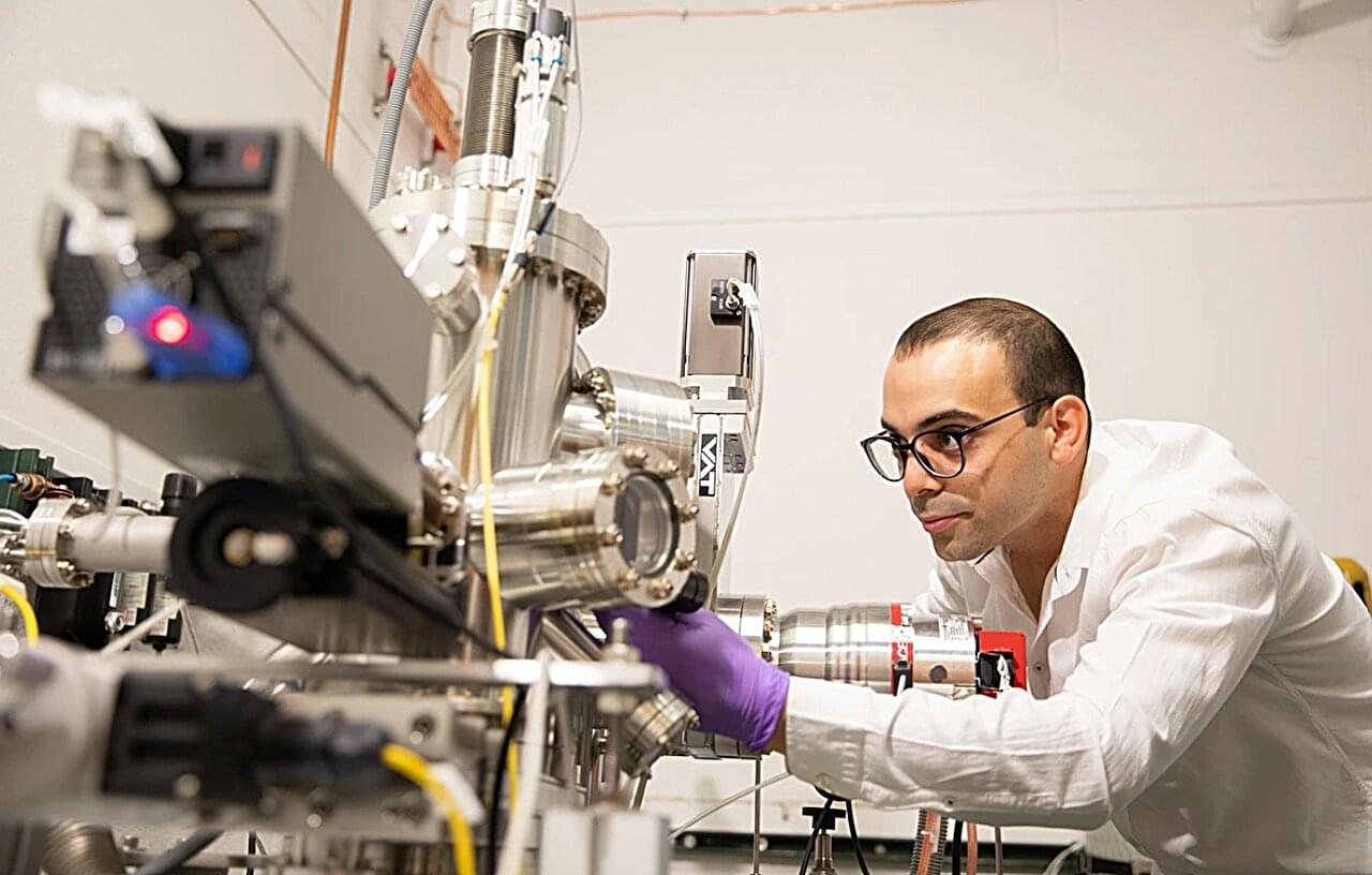
Turning molecules into reliable electronic devices with a new fabrication platform

Molecules are among the smallest building blocks available for making next-generation devices. Their unique, customizable properties enable promising applications in emerging computing, sensing, optical and quantum technologies.

But integrating molecules into functional devices at scale remains a challenge. Traditional semiconductor manufacturing processes can damage small, fragile molecular materials. Now, MIT researchers have developed a scalable fabrication technique that incorporates delicate molecular materials into electronic devices on a chip without causing damage.

Their method extends the capabilities of standard semiconductor manufacturing processes to accommodate molecules. The researchers first prefabricate the device components using traditional processes. Then, they introduce the molecules and harness nanoscale surface forces to mechanically transform the fabricated device, which self-assembles without damaging the molecules.

Pixel patterns harness diffraction for faster, more accurate nanoscale 3D printing

Researchers at the George W. Woodruff School of Mechanical Engineering have developed a new approach to nanoscale 3D printing that improves both speed and fidelity, overcoming a challenge that has limited the technology’s broader use in manufacturing.

Their work, led by Sourabh Saha, associate professor and Woodruff Faculty Fellow, and Harnjoo Kim, who conducted the research during his doctoral studies and later as a postdoctoral fellow in Saha’s lab, was recently published in the journal Nature Communications.

Nanoscale 3D printing allows researchers to create structures thousands of times smaller than the width of a human hair. These structures have potential applications in fields ranging from advanced computing and optics to biomedical devices and clean energy technologies. However, increasing printing speed often comes at the expense of quality.

Light controls nanoscale ‘bubble’ domains in a ferroelectric crystal

Researchers at Flinders University have discovered an unexpected way light can control tiny electronic structures inside advanced materials, a development that could help pave the way for more energy-efficient memory devices, sensors and future computing technologies.

The new study, involving experts from around the world, explores electronic properties and optical science to uncover new energy and material capabilities.

“We discovered that light can control nanoscale ‘bubble’ domains (about the size of just a few billionths of a meter across) inside a special ferroelectric crystal,” says Dr. Pankaj Sharma, senior lecturer in experimental condensed matter physics at Flinders University.

Ultrafast X-ray flashes partially reverse the damage they cause, enabling brighter, more accurate imaging

The interaction between X-rays and matter can be actively controlled, according to an international research team led by the University of Hamburg and SLAC National Accelerator Laboratory that has succeeded in producing bright X-ray images with significantly less damage. In an article published in Nature Communications, the researchers report using ultrafast pulses that partially reverse the damage they generate.

X-rays are ionizing radiation and can damage virtually all matter. That is why radiologists strive to keep the X-ray dose in imaging as low as possible. At the same time, they must ensure the image is bright enough and contains sufficient detail for diagnosis. This trade-off has shaped X-ray imaging for decades.

Researchers who want to image chemical reactions in individual molecules and nanoparticles face a far more extreme version of the same problem. To capture something as small and fleeting as a reaction within a cluster of atoms, they must illuminate the sample with a large number of X-ray photons in an extremely short burst. The most advanced tools for this—X-ray free-electron lasers (XFELs)—produce flashes short enough to “outrun” the physical destruction of the sample.

/* */