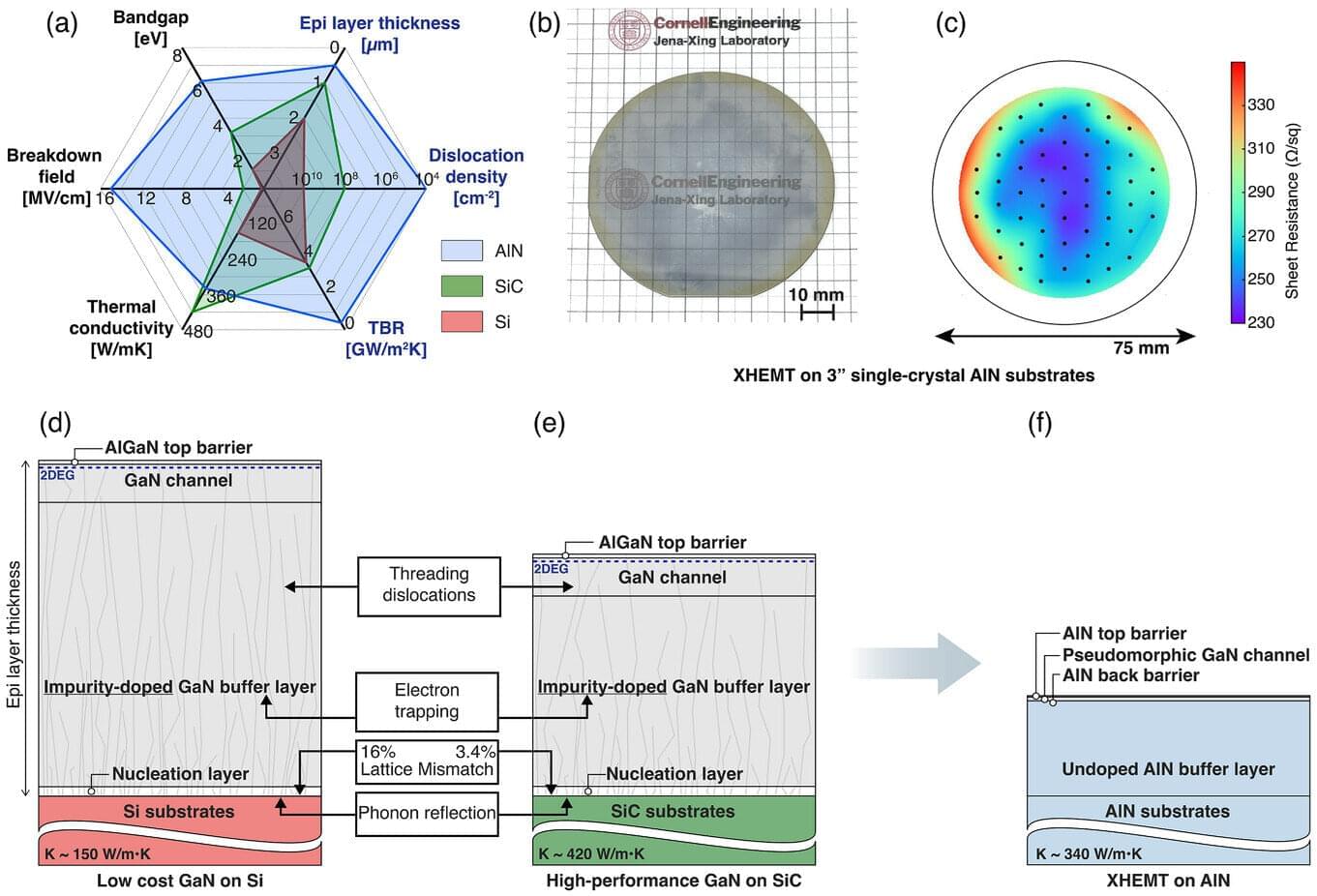
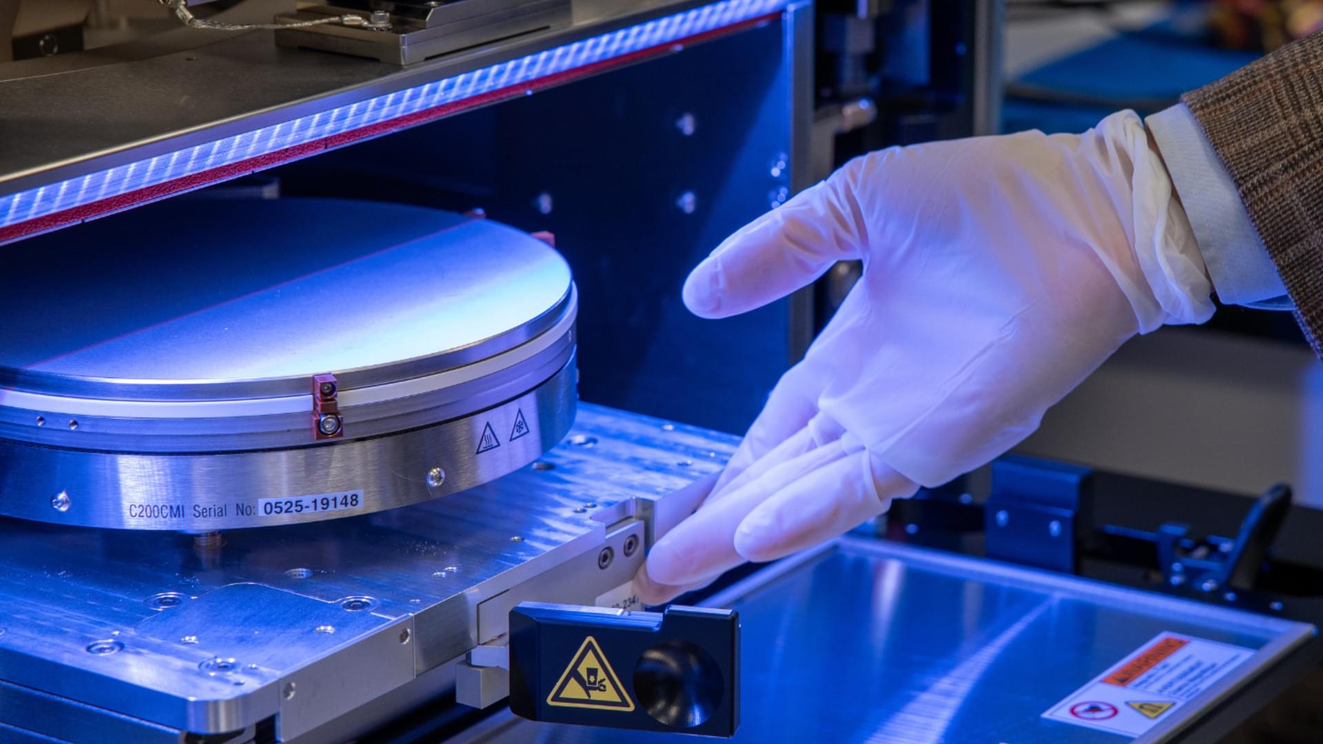
A U of A engineering researcher is using sunlight and semiconductor catalysts to produce hydrogen by splitting apart water molecules into their constituent elements.
“The process to form the semiconductor, called thermal condensation polymerization, uses cheap and Earth-abundant materials, and could eventually lead to a more efficient, economical path to clean energy than existing solar technologies,” says project lead Karthik Shankar of the Department of Electrical and Computer Engineering, an expert in the field of photocatalysis.
In a collaboration between the U of A and the Technical University of Munich, results of the research were published in the Journal of the American Chemical Society.
A UNSW study published today in Nature Communications presents an exciting step towards domain-wall nanoelectronics: a novel form of future electronics based on nano-scale conduction paths, and which could allow for extremely dense memory storage.
FLEET researchers at the UNSW School of Materials Science and Engineering have made an important step in solving the technology’s primary long-standing challenge of information stability.
A discovery by an international team of scientists has revealed room-temperature ferroelectric and resistive switching behaviors in single-element tellurium (Te) nanowires, paving the way for advancements in ultrahigh-density data storage and neuromorphic computing.
Published in Nature Communications, this research marks the first experimental evidence of ferroelectricity in Te nanowires, a single-element material, which was previously predicted only in theoretical models.
“Ferroelectric materials are substances that can store electrical charge and keep it even when the power is turned off, and their charge can be switched by applying an external electric field—a characteristic essential for non-volatile memory applications,” points out co-corresponding author of the paper Professor Yong P. Chen, a principal investigator at Tohoku University’s Advanced Institute for Materials Research (AIMR) and a professor at Purdue and Aarhus Universities.
However, when photons are contained within structures that are smaller than their wavelength, these measures collapse into each other, and so the definition is of total angular momentum (TAM). It’s this feature, only occurring for photons confined in this way, that has now been entangled for the first time.
Researchers at Technion-Israel Institute of Technology used gratings to confine photons within a circular or spiral nanoscale platform and mapped their states, entangling the TAMs of pairs of photons before scattering them to free space. Entangling TAMs might seem like a minor development, seeing that SAMs and OAMs have each been entangled before, but the authors write: “We observe that entanglement in TAM leads to a completely different structure of quantum correlations of photon pairs, compared with entanglement related to the two constituent angular momenta.”
Quantum entanglement is considered key to quantum computing. The authors propose their work could lead to information processing conducted using the entangled TAMs of photons confined to chips. Entangling TAMs allows quantum processors based around photons to be smaller than would be possible if one of the properties that only emerges under less confined conditions was used. That potentially enables the miniaturization of future quantum computers.
Researchers from Max Born Institute have demonstrated a successful way to control and manipulate nanoscale magnetic bits—the building blocks of digital data—using an ultrafast laser pulse and plasmonic gold nanostructures. The findings were published in Nano Letters.
All-optical, helicity-independent magnetization switching (AO-HIS) is one of the most interesting and promising mechanisms for this endeavor, where the magnetization state can be reversed between two directions with a single femtosecond laser pulse, serving as “0s” and “1s” without any external magnetic field or complex wiring. This opens up exciting possibilities for creating memory devices that are not only faster and more robust but also consume far less power.
Ultrafast light-driven control of magnetization on the nanometer-length scale is key to achieving competitive bit sizes in next-generation data storage technology. However, it is currently not well understood to what extent basic physics processes such as heat transfer at the nanoscale and the propagation of magnetic domain walls limit the minimum achievable bit size.
Ultrafast light-driven control of magnetization on the nanometer length scale is key to achieve competitive bit sizes in next generation data storage technology. Researchers at Max Born Institute in Berlin and of the large scale facility Elettra in Trieste, Italy, have successfully demonstrated the ultrafast emergence of all-optical switching by generating a nanometer scale grating by interference of two pulses in the extreme ultraviolet spectral range.
The physics of optically driven magnetization dynamics on the femtosecond time scale is of great interest for two main reasons: first, for a deeper understanding of the fundamental mechanisms of nonequilibrium, ultrafast spin dynamics and, second, for the potential application in the next generation of information technology with a vision to satisfy the need for both faster and more energy efficient data storage devices.
All–optical switching (AOS) is one of the most interesting and promising mechanisms for this endeavor, where the magnetization state can be reversed between two directions with a single femtosecond laser pulse, serving as “0s” and “1s.” While the understanding of the temporal control of AOS has progressed rapidly, knowledge on ultrafast transport phenomena on the nanoscale, important for the realization of all-optical magnetic reversal in technological applications, has remained limited due to the wavelength limitations of optical radiation. An elegant way to of overcoming these restrictions is to reduce the wavelengths to the extreme ultraviolet (XUV) spectral range in transient grating experiments. This technique is based on the interference of two XUV beams leading to a nanoscale excitation pattern and has been pioneered at the EIS-Timer beamline of the free-electron laser (FEL) FERMI in Trieste, Italy.
Human cyborgs are individuals who integrate advanced technology into their bodies, enhancing their physical or cognitive abilities. This fusion of man and machine blurs the line between science fiction and reality, raising questions about the future of humanity, ethics, and the limits of human potential. From bionic limbs to brain-computer interfaces, cyborg technology is rapidly evolving, pushing us closer to a world where humans and machines become one.
Researchers at MIT have developed a noninvasive medical monitoring device powerful enough to detect single cells within blood vessels, yet small enough to wear like a wristwatch. One important aspect of this wearable device is that it can enable continuous monitoring of circulating cells in the human body. The technology was reported in npj Biosensing.
The device—named CircTrek—was developed by researchers in the Nano-Cybernetic Biotrek research group, led by Deblina Sarkar, assistant professor at MIT and AT&T Career Development Chair at the MIT Media Lab. This technology could greatly facilitate early diagnosis of disease, detection of disease relapse, assessment of infection risk, and determination of whether a disease treatment is working, among other medical processes.
Whereas traditional blood tests are like a snapshot of a patient’s condition, CircTrek was designed to present real-time assessment, referred to in the npj Biosensing paper as having been “an unmet goal to date.” A different technology that offers monitoring of cells in the bloodstream with some continuity, in vivo flow cytometry, “requires a room-sized microscope, and patients need to be there for a long time,” says Kyuho Jang, a Ph.D. student in Sarkar’s lab.
If you haven’t heard of a tardigrade before, prepare to be wowed. These clumsy, eight-legged creatures, nicknamed water bears, are about half a millimeter long and can survive practically anything: freezing temperatures, near starvation, high pressure, radiation exposure, outer space and more. Researchers reporting in the journal Nano Letters took advantage of the tardigrade’s nearly indestructible nature and gave the critters tiny “tattoos” to test a microfabrication technique to build microscopic, biocompatible devices.
“Through this technology, we’re not just creating micro-tattoos on tardigrades—we’re extending this capability to various living organisms, including bacteria,” explains Ding Zhao, a co-author of the paper.
Microfabrication has revolutionized electronics and photonics, creating micro-and nanoscale devices ranging from microprocessors and solar cells to biosensors that detect food contamination or cancerous cells. But the technology could also advance medicine and biomedical engineering, if researchers can adapt microfabrication techniques to make them compatible with the biological realm.
Over the past decades, electronics engineers developed increasingly small, flexible and sophisticated sensors that can pick up a wide range of signals, ranging from human motions to heartrate and other biological signals. These sensors have in turn enabled the development of new electronics, including smartwatches, biomedical devices that can help monitor the health of users over time and other wearable or implantable systems.
Strain sensors, which are designed to convert mechanical force into electrical signals, are among the most widely used sensing devices within the electronics industry, as they can be valuable for tracking both human movements and health-related biological signals. While these sensors are already embedded in many electronic devices, most existing solutions are only able to track movements in one direction.
Sensors that can accurately pick up movements and forces in multiple directions could be highly advantageous, as they could be applied to a wider range of scenarios. In addition, these sensors could be embedded in existing electronic devices to broaden their functions or enhance their capabilities.