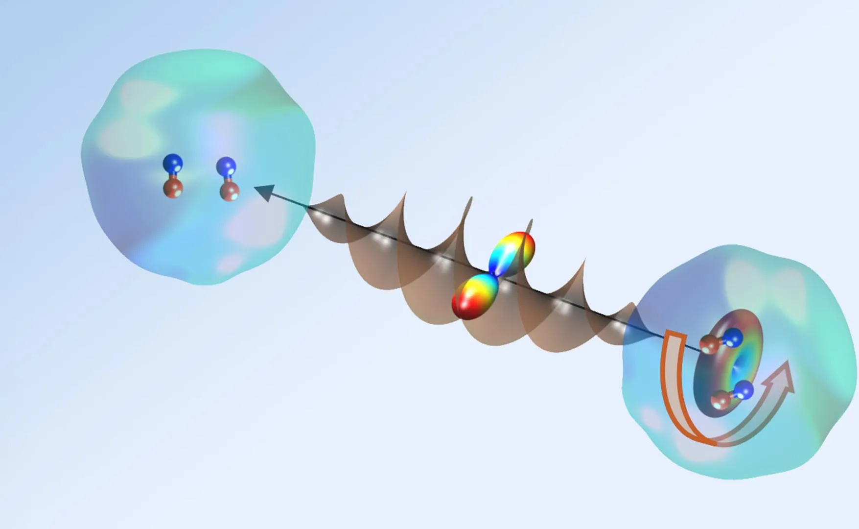
Toggle light / dark theme

Researchers have developed a new material that, by harnessing the power of sunlight, can clear water of dangerous pollutants. Created through a combination of soft chemistry gels and electrospinning—a technique where electrical force is applied to liquid to craft small fibers—the team constructed thin fiber-like strips of titanium dioxide (TiO₂), a compound often utilized in solar cells, gas sensors and various self-cleaning technologies.

Despite being a great alternative energy source, solar fuel systems that utilize TiO₂ nanoparticles are often power-limited because they can only undergo photocatalysis, or create , by absorbing non-visible UV light. This can cause significant challenges to implementation, including low efficiency and the need for complex filtration systems.

Yet when researchers added copper to the material to improve this process, their new structures, called nanomats, were able to absorb enough light energy to break down harmful pollutants in air and water, said Pelagia-Iren Gouma, lead author of the study and a professor of materials science and engineering at The Ohio State University.

Working at nanoscale dimensions, billionths of a meter in size, a team of scientists led by the Department of Energy’s Oak Ridge National Laboratory revealed a new way to measure high-speed fluctuations in magnetic materials. Knowledge obtained by these new measurements, published in Nano Letters, could be used to advance technologies ranging from traditional computing to the emerging field of quantum computing.

Many materials undergo phase transitions characterized by temperature-dependent stepwise changes of important fundamental properties. Understanding materials’ behavior near a critical transition temperature is key to developing new technologies that take advantage of unique physical properties. In this study, the team used a nanoscale quantum sensor to measure spin fluctuations near a phase transition in a magnetic thin film. Thin films with magnetic properties at room temperature are essential for data storage, sensors and electronic devices because their magnetic properties can be precisely controlled and manipulated.

The team used a specialized instrument called a scanning nitrogen-vacancy center microscope at the Center for Nanophase Materials Sciences, a DOE Office of Science user facility at ORNL. A nitrogen-vacancy center is an atomic-scale defect in diamond where a nitrogen atom takes the place of a carbon atom, and a neighboring carbon atom is missing, creating a special configuration of quantum spin states. In a nitrogen-vacancy center microscope, the defect reacts to static and fluctuating magnetic fields, allowing scientists to detect signals on a single spin level to examine nanoscale structures.

A new technology has been developed that enables the manufacturing of thin films, which typically require complex processes, using only water and oil in just one minute. Professor Kang Hee Ku and her research team from the School of Energy and Chemical Engineering at UNIST announced their novel process for creating catalytic thin films using oil droplets dispersed in water.

The developed technology involves a process in which nanomaterial precursors attached to the surface of oil droplets float to the surface of the water, where they assemble into a thin film. When is added, it decomposes due to the thin film precursors, producing gas bubbles that cause the precursors to be lifted and assembled on the water surface within one minute.

This process allows for precise control of the thin film thickness, adjustable from 350 μm, and enables the synthesis of thin films covering an area of up to 100 cm² using various raw materials. The resulting thin films exhibit a porous structure with a , featuring exceptional mechanical strength and flexibility.

Cadmium-based nanostructures are opening new possibilities in near-infrared (NIR) technology, from medical imaging to fiber optics and solar energy.

A major challenge in their development is controlling their atomic structure with precision, which researchers at HZDR and TU Dresden tackled using cation exchange. This technique allows for precise manipulation of nanostructure composition, unlocking new optical and electronic properties. The research highlights the crucial role of active corners and defects, which influence charge transport and light absorption. By linking these nanostructures into organized systems, scientists are paving the way for self-assembling materials with advanced functions, from improved sensors to next-generation electronics.

Harnessing Near-Infrared Light with Cadmium-Based Nanostructures.

Scientists have developed shape-shifting nanorobots that can flow like liquid and solidify like steel, paving the way for breakthroughs in medicine, engineering, and robotics. These nanobots, inspired by gallium-based materials, respond to magnetic fields, allowing them to navigate through tight spaces, repair electronics, and even perform medical procedures. While still in the early stages, this futuristic technology could lead to self-healing materials, autonomous repairs, and shape-adaptive robotics, bringing us closer to a world of smart, responsive materials.

For the first time, scientists have directly measured the cross-section of a weak r-process nuclear reaction using a radioactive ion beam. Specifically, the team studied the reaction 94Sr(α, n)97Zr, where a radioactive isotope of strontium (strontium-94) absorbs an alpha particle (a helium nucleus), emits a neutron, and becomes zirconium-97.

The findings have been published as an Editors’ Suggestion in Physical Review Letters

<em> Physical Review Letters (PRL)</em> is a prestigious peer-reviewed scientific journal published by the American Physical Society. Launched in 1958, it is renowned for its swift publication of short reports on significant fundamental research in all fields of physics. PRL serves as a venue for researchers to quickly share groundbreaking and innovative findings that can potentially shift or enhance understanding in areas such as particle physics, quantum mechanics, relativity, and condensed matter physics. The journal is highly regarded in the scientific community for its rigorous peer review process and its focus on high-impact papers that often provide foundational insights within the field of physics.

A study led by the University of Portsmouth has achieved unprecedented precision in detecting tiny shifts in light displacements at the nanoscale. This is relevant in the characterization of birefringent materials and in high-precision measurements of rotations.

The quantum sensing breakthrough is published in the journal Physical Review A, and has the potential to revolutionize many aspects of daily life, industry, and science.

Imagine two photons, massless particles of light, that are intertwined in a unique way, meaning their propagation is connected even when they are separated. When these photons pass through a device that splits the particles of light into two paths—known as a beam-splitter—they interfere with each other in special patterns. By analyzing these patterns, researchers have developed a highly precise method to detect even the tiniest initial spatial shifts between them.

Scientists from the RIKEN Center for Emergent Matter Science (CEMS) and collaborators have discovered a new way to control superconductivity—an essential phenomenon for developing more energy-efficient technologies and quantum computing—by simply twisting atomically thin layers within a layered device.

By adjusting the twist angle, they were able to finely tune the “superconducting gap,” which plays a key role in the behavior of these materials. The research is published in Nature Physics.

The superconducting gap is the energy threshold required to break apart Cooper pairs—bound electron pairs that enable superconductivity at low temperatures. Having a larger gap allows superconductivity to persist at higher, more accessible temperatures, and tuning the gap is also important for optimizing Cooper pair behavior at the nanoscale, contributing to the high functionality of quantum devices.

Memory engrams are formed through experience-dependent plasticity of neural circuits, but their detailed architectures remain unresolved. Using three-dimensional electron microscopy, we performed nanoscale reconstructions of the hippocampal CA3-CA1 pathway after chemogenetic labeling of cellular ensembles recruited during associative learning. Neurons with a remote history of activity coinciding with memory acquisition showed no strong preference for wiring with each other. Instead, their connectomes expanded through multisynaptic boutons independently of the coactivation state of postsynaptic partners. The rewiring of ensembles representing an initial engram was accompanied by input-specific, spatially restricted upscaling of individual synapses, as well as remodeling of mitochondria, smooth endoplasmic reticulum, and interactions with astrocytes.