Toggle light / dark theme

As computer chips continue to get smaller and more complex, the ultrathin metallic wires that carry electrical signals within these chips have become a weak link. Standard metal wires get worse at conducting electricity as they get thinner, ultimately limiting the size, efficiency, and performance of nanoscale electronics.

In a paper published in Science, Stanford researchers show that niobium phosphide can conduct electricity better than copper in films that are only a few atoms thick. Moreover, these films can be created and deposited at sufficiently low temperatures to be compatible with modern computer chip fabrication. Their work could help make future electronics more powerful and more energy efficient.

“We are breaking a fundamental bottleneck of traditional materials like copper,” said Asir Intisar Khan, who received his doctorate from Stanford and is now a visiting postdoctoral scholar and first author on the paper.

A groundbreaking step in quantum technology has been achieved with the demonstration of an integrated spin-wave quantum memory, overcoming challenges of photon transmission loss and noise suppression.

Quantum memories play a crucial role in creating large-scale quantum networks by enabling the connection of multiple short-distance entanglements into long-distance entanglements. This approach helps to overcome photon transmission losses effectively. Rare-earth ion-doped crystals are a promising candidate for implementing high-performance quantum memories, and integrated solid-state quantum memories have already been successfully demonstrated using advanced micro-and nano-fabrication techniques.

Limitations of Existing Quantum Memory.

Conventional photonic devices exhibit static optical properties that are design-dependent, including the material’s refractive index and geometrical parameters. However, they still possess attractive optical responses for applications and are already exploited in devices across various fields. Hydrogel photonics has emerged as a promising solution in the field of active photonics by providing primarily deformable geometric parameters in response to external stimuli. Over the past few years, various studies have been undertaken to attain stimuli-responsive photonic devices with tunable optical properties. Herein, we focus on the recent advancements in hydrogel-based photonics and micro/nanofabrication techniques for hydrogels. In particular, fabrication techniques for hydrogel photonic devices are categorized into film growth, photolithography (PL), electron-beam lithography (EBL), and nanoimprint lithography (NIL). Furthermore, we provide insights into future directions and prospects for deformable hydrogel photonics, along with their potential practical applications.


Microsystems & Nanoengineering volume 10, Article number: 1 (2024) Cite this article.

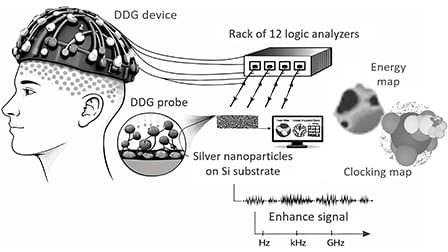
Scientists recreated molecular switches that regulate biological timing, aiding nanotechnology and explaining evolutionary advantages.

Living organisms monitor time – and react to it – in many different ways, from detecting light and sound in microseconds to responding physiologically in pre-programmed ways, via their daily sleep cycle, monthly menstrual cycle, or to changes in the seasons.

These time-sensitive reactions are enabled by molecular switches or nanomachines that function as precise molecular timers, programmed to activate or deactivate in response to environmental cues and time intervals.

A team of materials scientists, physicists, mechanical engineers, and molecular physiologists at Stanford University have developed a nanoparticle technique that can be used to measure force dynamics inside a living creature, such as Caenorhabditis elegans worms biting their food.

In their paper published in the journal Nature, the group describes how they used to excite luminescent nanocrystals in a way that allowed the energy levels of cells inside a C. elegans worm to be measured.

Andries Meijerink, with Utrecht University, has published a News & Views piece in the same journal issue, outlining the work done by the team in California.

Mechanical force is an essential feature for many physical and biological processes. Remote measurement of mechanical signals with high sensitivity and spatial resolution is needed for a wide range of applications, from robotics to cellular biophysics and medicine and even to space travel. Nanoscale luminescent force sensors excel at measuring piconewton forces, while larger sensors have proven powerful in probing micronewton forces.

However, large gaps remain in the force magnitudes that can be probed remotely from subsurface or interfacial sites, and no individual, non-invasive sensor has yet been able to make measurements over the large dynamic range needed to understand many systems.

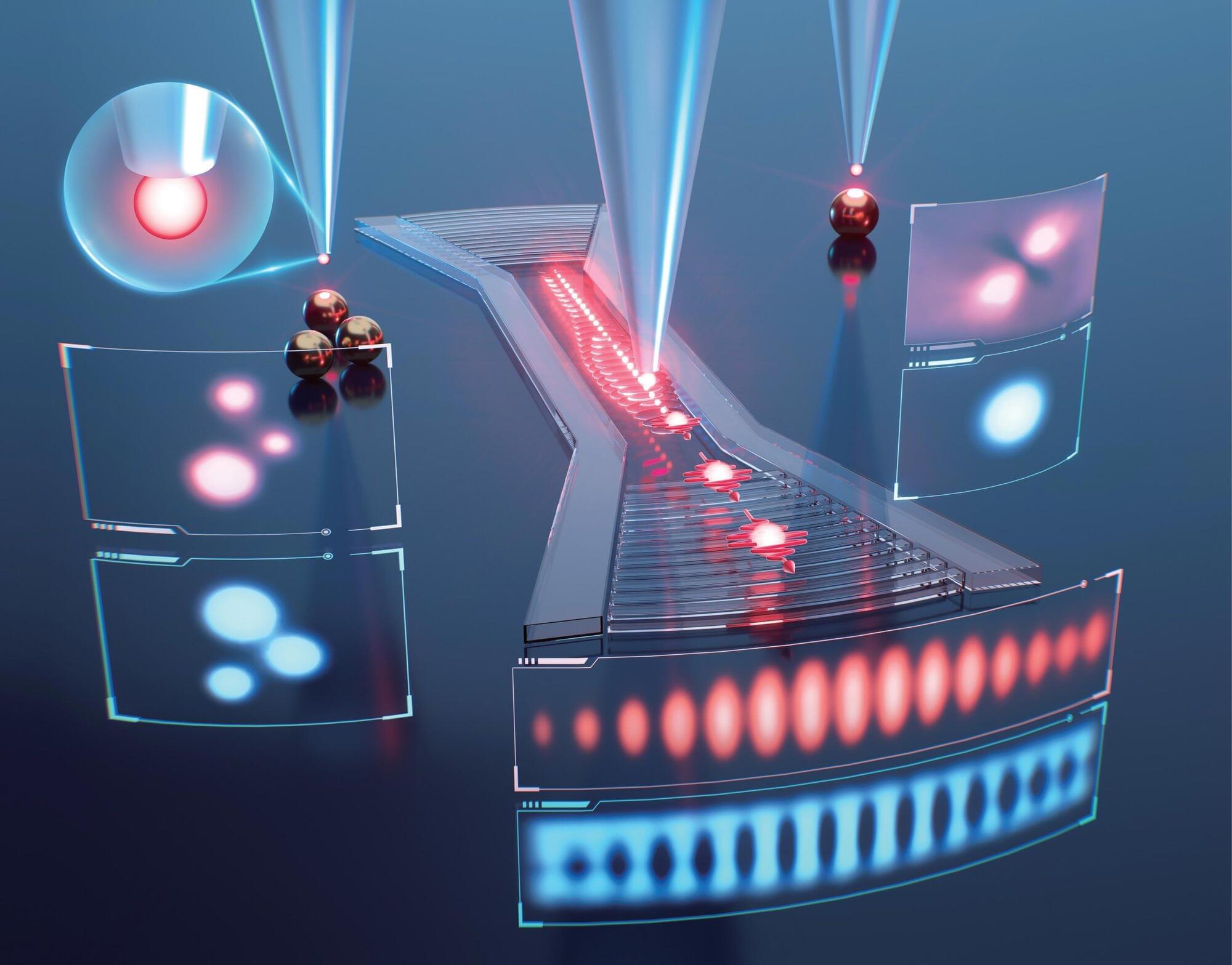
A groundbreaking technique using time-resolved electron microscopy and multi-polarization lasers has allowed scientists to analyze plasmonic waves with great precision.

This method helped uncover the stable and dynamic nature of meron pairs’ spin textures, opening new avenues in nanoscale technology.

Advancing Plasmonics with Multi-Polarization Laser Techniques.

Penn Engineers have modified lipid nanoparticles (LNPs) — the revolutionary technology behind the COVID-19 mRNA vaccines — to not only cross the blood-brain barrier (BBB) but also to target specific types of cells, including neurons. This breakthrough marks a significant step toward potential next-generation treatments for neurological diseases like Alzheimer’s and Parkinson’s.

In a new paper in Nano Letters, the researchers demonstrate how peptides — short strings of amino acids — can serve as precise targeting molecules, enabling LNPs to deliver mRNA specifically to the endothelial cells that line the blood vessels of the brain, as well as neurons.

This represents an important advance in delivering mRNA to the cell types that would be key in treating neurodegenerative diseases; any such treatments will need to ensure that mRNA arrives at the correct location. Previous work by the same researchers proved that LNPs can cross the BBB and deliver mRNA to the brain, but did not attempt to control which cells the LNPs targeted.

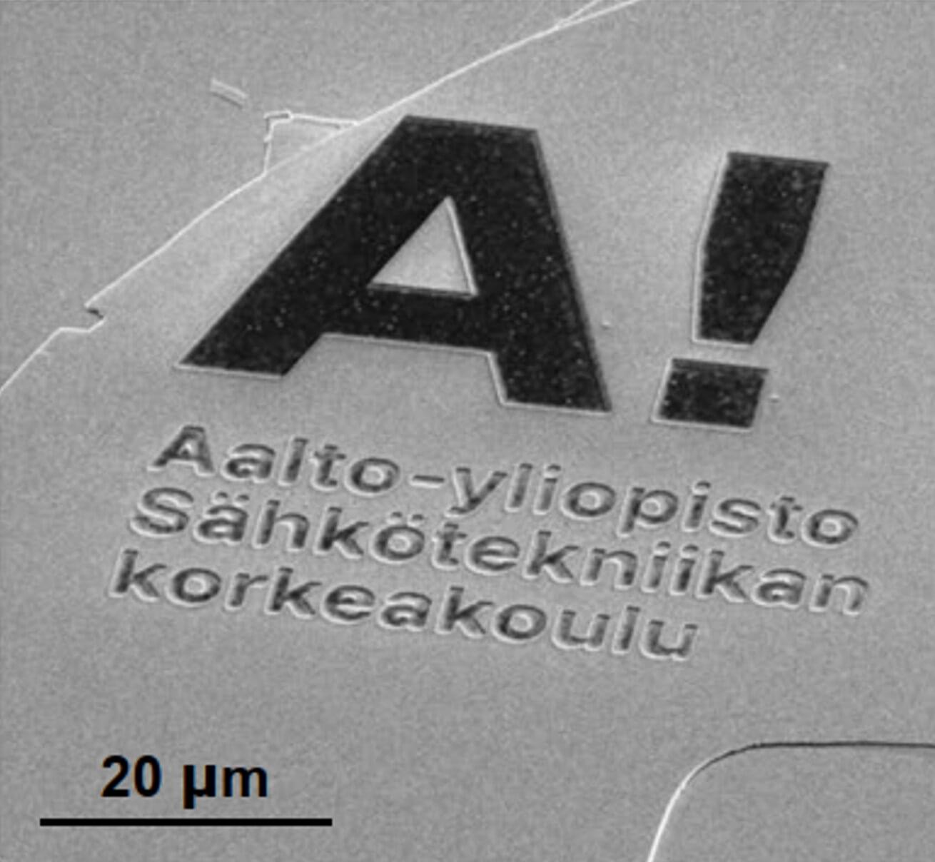
In a breakthrough set to revolutionize the semiconductor industry, the School of Engineering of the Hong Kong University of Science and Technology (HKUST) has developed the world’s first-of-its-kind deep-ultraviolet (UVC) microLED display array for lithography machines. This enhanced efficiency UVC microLED has showcased the viability of a lowered cost maskless photolithography through the provision of adequate light output power density, enabling exposure of photoresist films in a shorter time.

Conducted under the supervision of Prof. Kwok Hoi-Sing, Founding Director of the State Key Laboratory of Advanced Displays and Optoelectronics Technologies at HKUST, the study was a collaborative effort with the Southern University of Science and Technology, and the Suzhou Institute of Nanotechnology of the Chinese Academy of Sciences.

A lithography machine is crucial equipment for semiconductor manufacturing, applying short-wavelength ultraviolet light to make integrated circuit chips with various layouts. However, traditional mercury lamps and deep ultraviolet LED light sources have shortcomings such as large device size, low resolution, high energy consumption, low light efficiency, and insufficient optical power density.

Living organisms monitor time—and react to it—in many different ways, from detecting light and sound in microseconds to responding physiologically in pre-programmed ways, via their daily sleep cycle, monthly menstrual cycle, or to changes in the seasons.

Such an ability to react at different timescales is made possible via molecular switches or nanomachines that act or communicate as precise molecular timers, programmed to turn on and off in response to the environment and time.

Now, scientists at Université de Montréal have successfully recreated and validated two distinct mechanisms that can program both the activation and deactivation rates of nanomachines in living organisms across multiple timescales.