In the current issue of the journal Nature Methods, siibra is introduced as a software suite that integrates data from different multimodal sources into a comprehensive atlas of the human brain and makes the data easily accessible—for interactive exploration and automated, reproducible data analyses, simulations and AI applications. siibra is developed by an international team of scientists led by the Institute of Neuroscience and Medicine (INM-1) at Forschungszentrum Jülich.
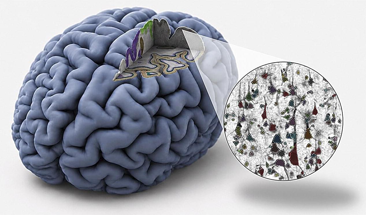
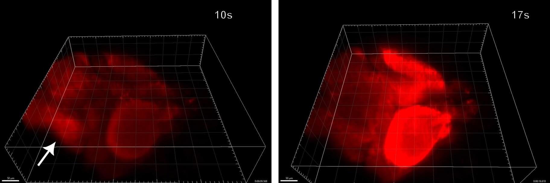
To better understand the human brain, information from various levels must be integrated, from molecules and cells to their organization and entire networks. A central challenge is that these data are often scattered across sources and organized differently. They originate from methods such as microscopy, MRI and connectivity analysis; exist in formats ranging from images to tables; and rely on different spatial reference systems and conceptual taxonomies.
“Using siibra, we are now able to access and analyze brain data in a structured way from micro-to macrolevels—for more precise neuroscience studies, bio-inspired AI and clinical applications such as deep brain stimulation,” says Dr. Timo Dickscheid, working group leader for “Big Data Analytics.”