In quantum mechanics, the geometry of quantum states has emerged as a powerful framework for understanding phenomena ranging from electrical conductivity to superconductivity. One research direction aims to extend these geometric concepts to non-Hermitian quantum mechanics—where systems can exchange energy with their environment—including the generalization of the Berry phase, a key geometric quantity, to the non-Hermitian case.
However, many geometric properties unique to non-Hermitian quantum mechanics remain poorly understood.
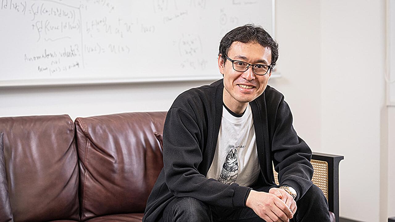
“We knew geometry played a central role in ordinary quantum mechanics, but what genuinely new geometric effects might emerge in the non-Hermitian case was far from clear,” explains Tomoki Ozawa, a theoretical physicist at AIMR. “We wanted to identify geometric phenomena that are truly intrinsic to non-Hermitian quantum mechanics.”
Go to https://ground.news/sabine to get 40% off the Vantage plan and see through sensationalized reporting. Stay fully informed on events around the world with Ground News.
The #1 most-wanted particle in physics is the graviton, a quantum of gravity. If physicists were to prove that gravitons exist, they would unambiguously prove that Einstein’s theory is ultimately wrong and must be replaced by a more complete theory that gives quantum properties to space and time. In a recent paper, a physicist came up with an ingenious experiment that could prove that gravitons do exist. Let’s take a look.
A new quantum computing chip turns destructive noise into a programmable feature, helping scientists study signal loss and error correction to build more effective systems in the future.
Stanford researchers may have just opened the door to a future where quantum technology no longer depends on multi-million-dollar cryogenic systems.
In this video, we break down Stanford University’s groundbreaking 2025 research that demonstrated room-temperature photon-electron quantum entanglement on a silicon-compatible chip. While this is not yet a full quantum computer, it represents a major step toward solving one of the biggest challenges in quantum technology: the extreme cooling requirements that have limited quantum systems for decades.
We’ll explore how twisted light, molybdenum diselenide (MoSe₂), valley states, and silicon nanostructures work together to create stable quantum interactions without dilution refrigerators operating near absolute zero. You’ll also learn what this breakthrough means for the future of quantum computing, quantum communication, quantum cryptography, and the emerging quantum internet.
🔹 What Stanford actually built. 🔹 Why current quantum computers require ultra-cold temperatures. 🔹 How room-temperature quantum entanglement was achieved. 🔹 The role of twisted photons and valley states. 🔹 What this breakthrough can and cannot do today. 🔹 Potential impact on IBM, Google, Microsoft, IonQ, and the broader quantum industry. 🔹 The future of room-temperature quantum networks and computing.
If this technology successfully scales, it could dramatically reduce the cost, complexity, and energy requirements of quantum systems, potentially transforming quantum technology from a specialized laboratory tool into a widely deployable platform.
Subscribe for in-depth analysis of emerging technologies, quantum computing breakthroughs, artificial intelligence, geopolitics, defense innovation, and the technologies shaping the future.
Quantum computing could transform medicine, cybersecurity, clean energy and countless other industries, with Ottawa playing a leading role in the technology’s development. CTV’s Austin Lee reports that researchers at the University of Ottawa and local cybersecurity companies are helping prepare for the quantum era. Experts say quantum computers will solve complex problems dramatically faster than today’s computers but could also threaten current encryption methods. Ottawa-based companies are already developing quantum-safe cybersecurity technologies to protect future digital infrastructure.
CTV News on TikTok: https://www.tiktok.com/discover/CTV-News. CTV News on X (formerly Twitter): / ctvnews. CTV News on Reddit: / ctvnews. CTV News on LinkedIn: / ctv-news.
– CTV News is Canada’s most-watched news organization both locally and nationally, and has a network of national, international, and local news operations.
🚀 *Harvard says quantum computers are a decade ahead of schedule—and the evidence is arriving faster than anyone expected.* ⚛️
QuEra’s new roadmap, its partnership with Amazon Braket, and Harvard’s latest breakthroughs are reshaping the future of quantum computing. In this video, we break down why leading researchers now believe fault-tolerant quantum computers could arrive years earlier than predicted, what QuEra’s Libra system means, and how cloud-accessible quantum computing could transform industries like drug discovery, materials science, artificial intelligence, cybersecurity, and finance.
You’ll discover: 🔹 Why Harvard says the quantum timeline has accelerated by nearly a decade. 🔹 What QuEra’s 256 logical-qubit Libra system will actually do. 🔹 Why Amazon is betting on cloud-based fault-tolerant quantum computing by 2028 🔹 The difference between physical qubits and logical qubits. 🔹 How quantum error correction changed everything. 🔹 Why neutral-atom quantum computers are challenging IBM and Google. 🔹 The commercial race between QuEra, IBM, Microsoft, Quantinuum, and other quantum leaders. 🔹 What these breakthroughs mean for the future of encryption, AI, scientific research, and national security.
If you’re interested in quantum computing, emerging technologies, artificial intelligence, geopolitics, and the future of science, this channel brings you deeply researched, easy-to-understand explanations of the world’s biggest technological breakthroughs.
👍 If you enjoyed the video, don’t forget to *Like**, **Subscribe**, and **Turn On Notifications* so you never miss our latest updates on quantum technology and the future of computing.
A new scientific breakthrough has reignited one of the biggest debates in modern computing after researchers announced results suggesting that a quantum computer outperformed a classical supercomputer on a highly specialized task. The findings have fueled discussions about whether the era of \.
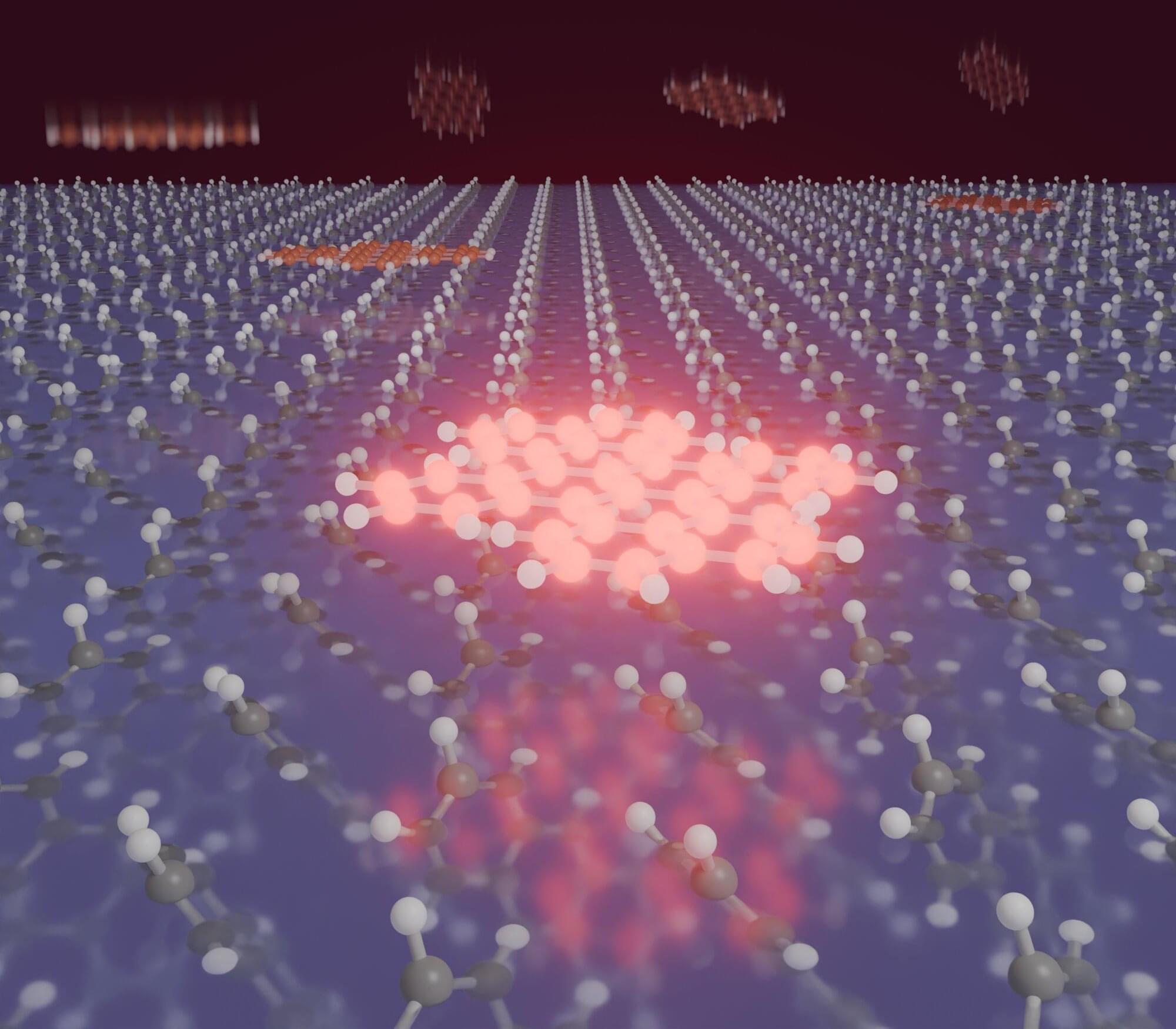
Scientists at the Max Planck Institute for the Science of Light (MPL) have developed a technique for interrogating molecules on surfaces with spectroscopic precision, thereby reaching the ultimate quantum limit for the first time. With their findings, published in Science, the researchers open new opportunities for the study of molecule-surface interactions and molecular quantum technologies.
Many optical quantum technologies rely on nanoscale objects, such as atoms or molecules, that interact strongly with light. These quantum emitters are used for generating single photons, storing quantum information and entanglement distribution, processes that find application in quantum communication and computation.
To investigate these emitters individually, researchers need to keep them in one place for a long time. This is usually achieved by either trapping them in a vacuum or placing them inside a bulk material. Quantum emitters located on a surface would create new opportunities to manipulate their functionalities by “touching them,” for example, with an atomically sharp tip, as is used in scanning tunneling microscopy (STM) and atomic force microscopy (AFM).
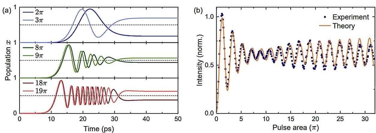
Physicists at Paderborn University have, for the first time, experimentally demonstrated the so-called “return” of Rabi oscillations in semiconductor quantum dots. The phenomenon, which was first predicted theoretically in 2007, describes the decrease in the emission intensity of the quantum dots, which are initially damped by interactions with the lattice vibrations of a solid (phonons).
Only through sufficiently strong optical excitation can the original intensity be restored and the oscillation “reawakened”—an effect that previously existed only in idealized theoretical models and has now been proven.
The results, published in Physical Review Letters, mark a decisive step toward scalable quantum applications.