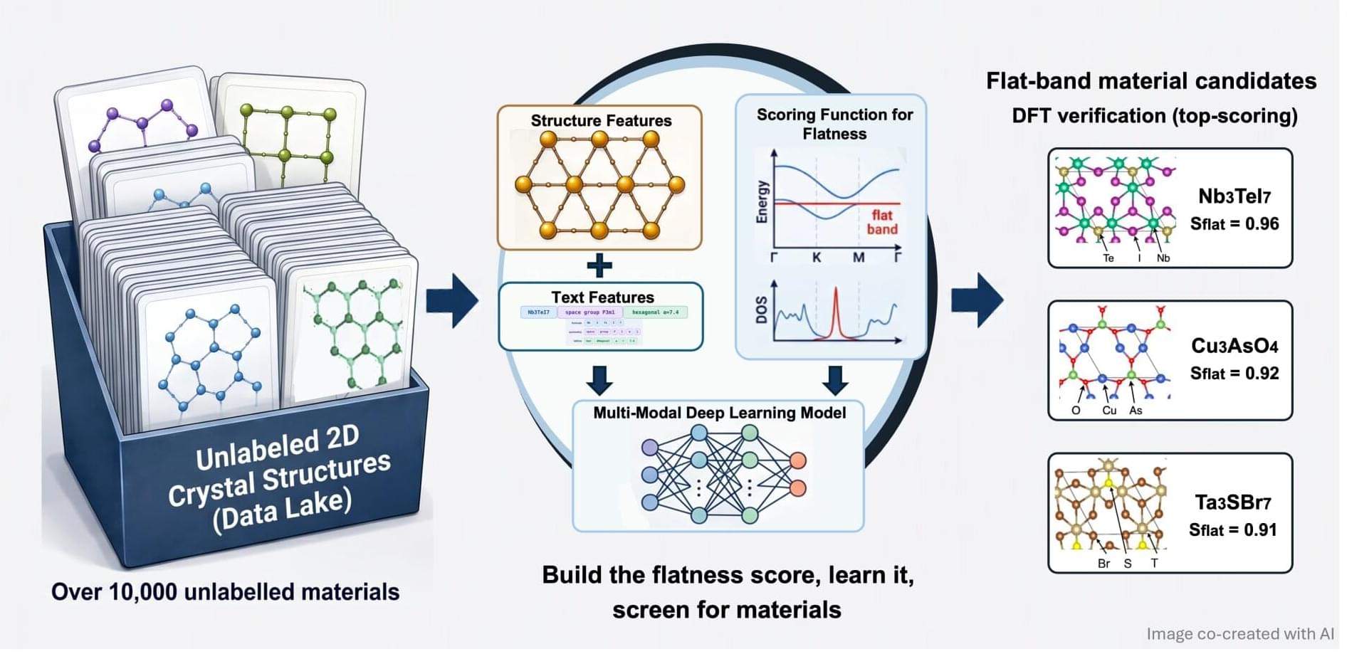
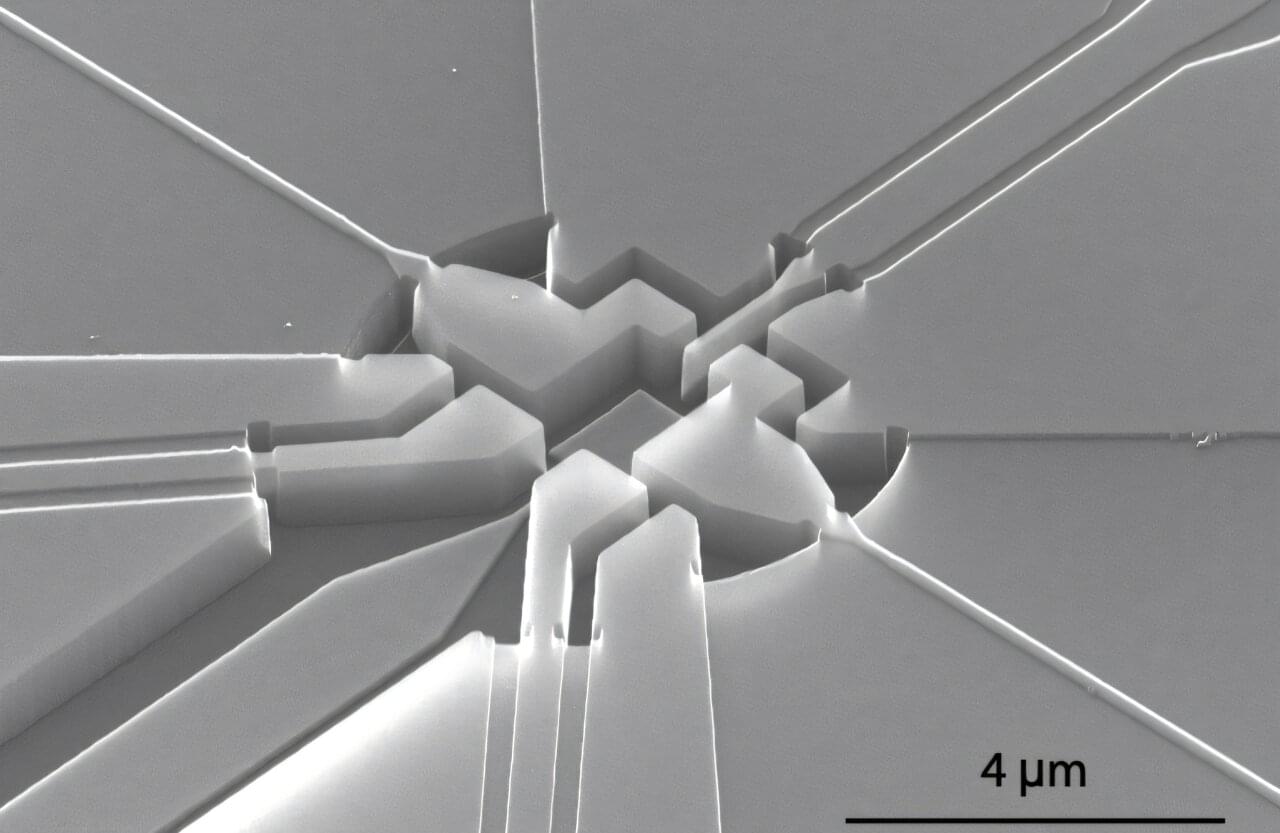
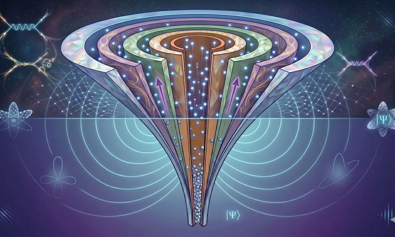
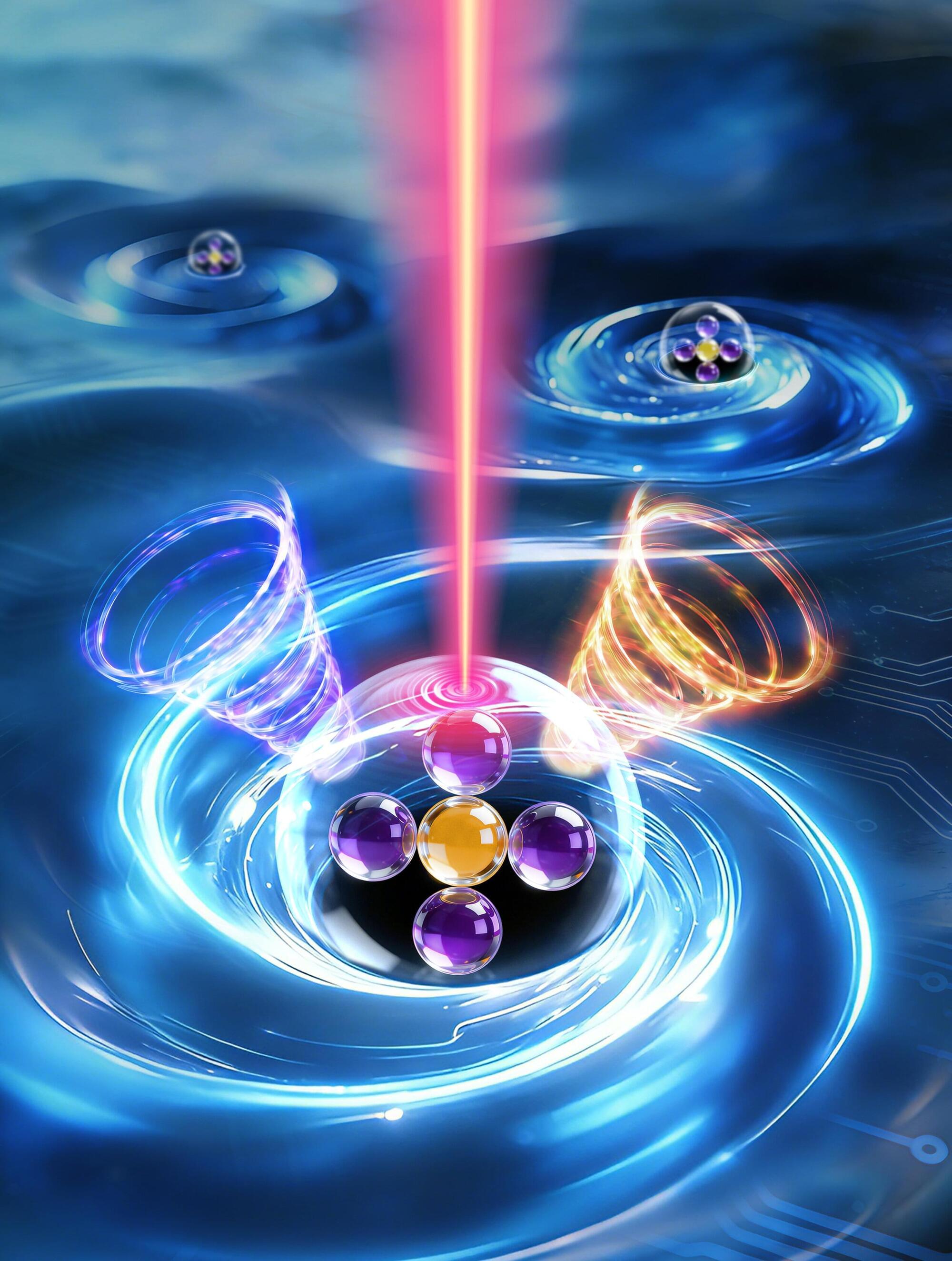
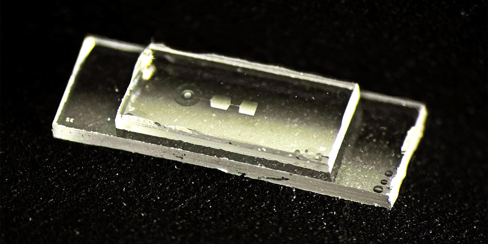
Toggle light / dark theme

Many next-generation quantum devices rely on single-photon emitters based on optically active defects in solids, known as color centers. Understanding their properties is fundamental to developing novel quantum technologies.

Now, in a study published in APL Materials, a multi-institutional research team led by Osaka University has sought to clarify the origin of the extremely bright color centers at the interface between (SiO2) and silicon carbide (SiC).

Previous research has demonstrated a range of factors that can play a role in the formation of these interface color centers, including the effect of annealing after oxidation. However, the energy level structure (i.e., the electronic transitions taking place) responsible for luminescence, a crucial factor for understanding the origin of color centers, was completely unknown.

A new formula that connects a material’s magnetic permeability to spin dynamics has been derived and tested 84 years after the debut of its electric counterpart.

If antiferromagnets, altermagnets, and other emerging quantum materials are to be harnessed for spintronic devices, physicists will need to better understand the spin dynamics in these materials. One possible path forward is to exploit the duality between electric and magnetic dynamics expressed by Maxwell’s equations. From this duality, one could naively expect mirror-like similarities in the behavior of electric and magnetic dipoles. However, a profound difference between the quantized lattice electric excitations—such as phonons—and spin excitations—such as paramagnetic and antiferromagnetic spin resonances and magnons—has now been unveiled in terms of their corresponding contributions to the static electric susceptibility and magnetic permeability. Viktor Rindert of Lund University in Sweden and his collaborators have derived and verified a formula that relates a material’s magnetic permeability to the frequencies of magnetic spin resonances [1].

Scientists have unlocked a new understanding of mesoporous silicon, a nanostructured version of the well-known semiconductor. Unlike standard silicon, its countless tiny pores give it unique electrical and thermal properties, opening up potential applications in biosensors, thermal insulation, photovoltaics, and even quantum computing.

Performing computation using quantum-mechanical phenomena such as superposition and entanglement.

Quantum computers could be made with fewer overall components, thanks to technology inspired by Schrödinger’s cat. A team of researchers from Amazon Web Services has used “bosonic cat qubits,” to improve the ability of quantum computers to correct errors. The demonstration of quantum error correction requiring reduced hardware overheads is reported in a paper published in Nature.

The system uses so-called cat (qubits are the quantum equivalent to classical computing bits), which are designed to be resistant against certain types of noise and errors that might disrupt the output of quantum systems. This approach requires fewer overall components to achieve quantum error correction than other designs.

Quantum computers are prone to errors, which limits their potential to exceed the capabilities of classical computers at certain tasks. Quantum error correction is a method that helps reduce errors by spreading information over multiple qubits, allowing the identification and correction of errors without corrupting the computation. However, most approaches to quantum error correction typically rely on a large number of additional qubits to provide sufficient protection against errors, potentially leading to an overall decrease in efficiency.

Laying the groundwork for quantum communication systems of the future, engineers at Caltech have demonstrated the successful operation of a quantum network of two nodes, each containing multiple quantum bits, or qubits—the fundamental information-storing building blocks of quantum computers.

To achieve this, the researchers developed a new protocol for distributing in a parallel manner, effectively creating multiple channels for sending data, or multiplexing. The work was accomplished by embedding ytterbium atoms inside crystals and coupling them to optical cavities—nanoscale structures that capture and guide light. This platform has unique properties that make it ideal for using multiple qubits to transmit quantum information-carrying photons in parallel.

“This is the first-ever demonstration of entanglement multiplexing in a quantum network of individual spin qubits,” says Andrei Faraon (BS ‘04), the William L. Valentine Professor of Applied Physics and Electrical Engineering at Caltech. “This method significantly boosts quantum communication rates between nodes, representing a major leap in the field.”

Researchers at the National Graphene Institute at the University of Manchester have achieved a significant milestone in the field of quantum electronics with their latest study on spin injection in graphene. The paper, published recently in Communications Materials, outlines advancements in spintronics and quantum transport.

Spin electronics, or spintronics, represents a revolutionary alternative to traditional electronics by utilizing the spin of electrons rather than their charge to transfer and store information. This method promises energy-efficient and high-speed solutions that exceed the limitations of classical computation, for next generation classical and quantum computation.

The Manchester team, led by Dr. Ivan Vera-Marun, has fully encapsulated in , an insulating and atomically flat 2D material, to protect its high quality. By engineering the 2D material stack to expose only the edges of , and laying magnetic nanowire electrodes over the stack, they successfully form one-dimensional (1D) contacts.

A new study from the University of Eastern Finland (UEF) explores the behavior of photons, the elementary particles of light, as they encounter boundaries where material properties change rapidly over time. This research uncovers remarkable quantum optical phenomena that may enhance quantum technology and paves the road for an exciting nascent field: four-dimensional quantum optics.

Four-dimensional optics is a research area investigating light scattering from structures which change in time and space. It holds immense promise for advancing microwave and optical technologies by enabling functionalities such as frequency conversion, amplification, polarization engineering and asymmetric scattering. That is why it has captured the interest of many researchers across the globe.

Previous years have seen significant strides in this area. For instance, a 2024 study published in Nature Photonics and also involving UEF highlights how incorporating optical features like resonances can drastically influence the interaction of electromagnetic fields with time-varying two-dimensional structures, opening exotic possibilities to control light.