Researchers have created a compact chip that manipulates light-based quantum information with remarkable precision, advancing the development of next-generation photonic and quantum technologies.
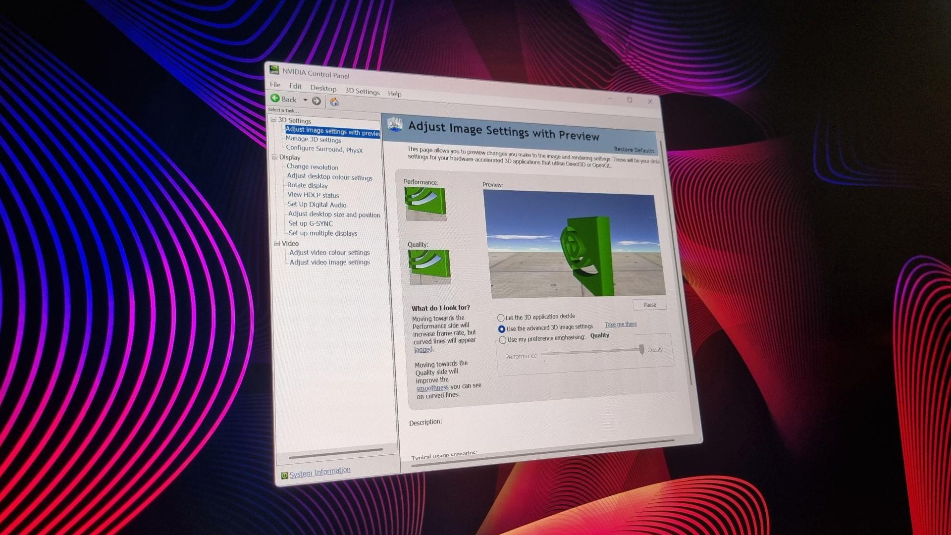
And two, the Nvidia App can be quite an online-focused affair in a way the old Control Panel was not. Besides the greyed-out checkbox in the Privacy settings labelled “required data” (something Nvidia explains is “Data that is necessary for Nvidia App to operate and cannot be switched off”), it can also lag quite badly on an unstable connection. In my personal experience, anyway.
Still, change comes for us all. I’ll miss the Control Panel’s classic rotating 3D image preview, the charmingly old-school HDCP menu that shows a rendering of an ancient Nvidia GPU plugged into what looks suspiciously like a plasma TV, and of course, the old Global Settings and Program Settings tabs with all of their many intricacies.
But is it progress? Perhaps. You can pry the Windows Control Panel from my cold, dead hands, though. That old clunker simply refuses to die, although I don’t think it’ll be that long before I write a similar obituary.
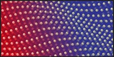
Temperature is a tuning knob for semiconductor-band-gap energies, which in turn play a key role in the performance of optoelectronic devices. But computational tools for predicting this temperature dependence from first principles struggle to capture the influence of one main factor: many-electron effects in electron–phonon interactions. Xiaoxun Gong at the University of California, Berkeley, and colleagues now demonstrate a computational framework that properly accounts for these effects [1]. Their framework could aid the design of materials and devices with precisely tailored electronic and optical properties.
Theoretical calculations consistently underestimate the strength of electron–phonon interactions and how they modify band gaps at different temperatures. Previous studies indicated that this discrepancy likely stems from insufficient treatment of many-electron effects. To quantify the role of electron–phonon interactions more accurately, Gong and his colleagues have proposed a new framework that breaks down the total temperature-dependent modification of the band gap into various contributions. Within this framework, they analyzed electron–phonon interactions using a many-body perturbation theory, in which electrons’ energies and their perturbation by phonons are captured by the “GW” approximation.
To test their framework, the researchers computed the band gaps of diamond, silicon, and gallium phosphide at different temperatures. They found that the temperature-dependent band-gap modification was enhanced using the GW-based perturbation theory—especially compared to a description based on density-functional theory (DFT), the workhorse tool for first-principles electronic calculations. The new predictions for all three materials showed excellent agreement with previous measurements.
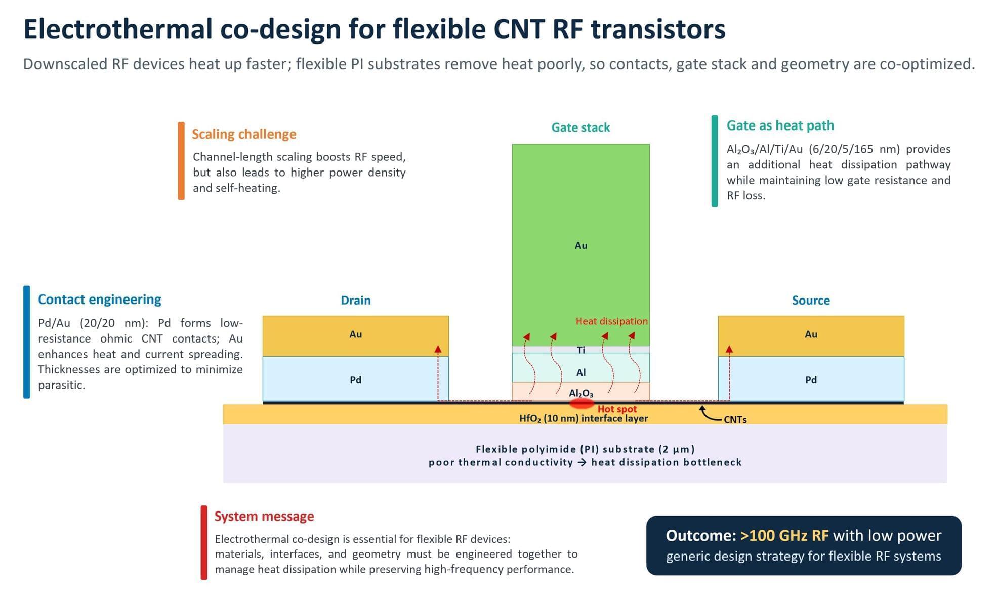
Over the past decades, electronics engineers worldwide have been trying to develop devices that could enable even faster communications between devices, all while consuming less energy. To meet the demands of the sixth generation (6G) of wireless communication technology, these devices should operate at frequencies above 100 gigahertz (GHz).
So far, developing flexible electronic components that can operate at these high frequencies while consuming little power has proved challenging. One promising approach for fabricating these devices entails the use of carbon nanotubes (CNTs), extremely thin and cylindrical structures with advantageous electrical and thermal properties.
Researchers at Peking University and Stanford University recently developed new flexible and low-power CNT-based transistors that operate at frequencies above 100 GHz. These transistors, presented in a paper published in Nature Electronics, could potentially help to speed up communications between future smartphones, sensors, wearable devices, and other flexible devices.
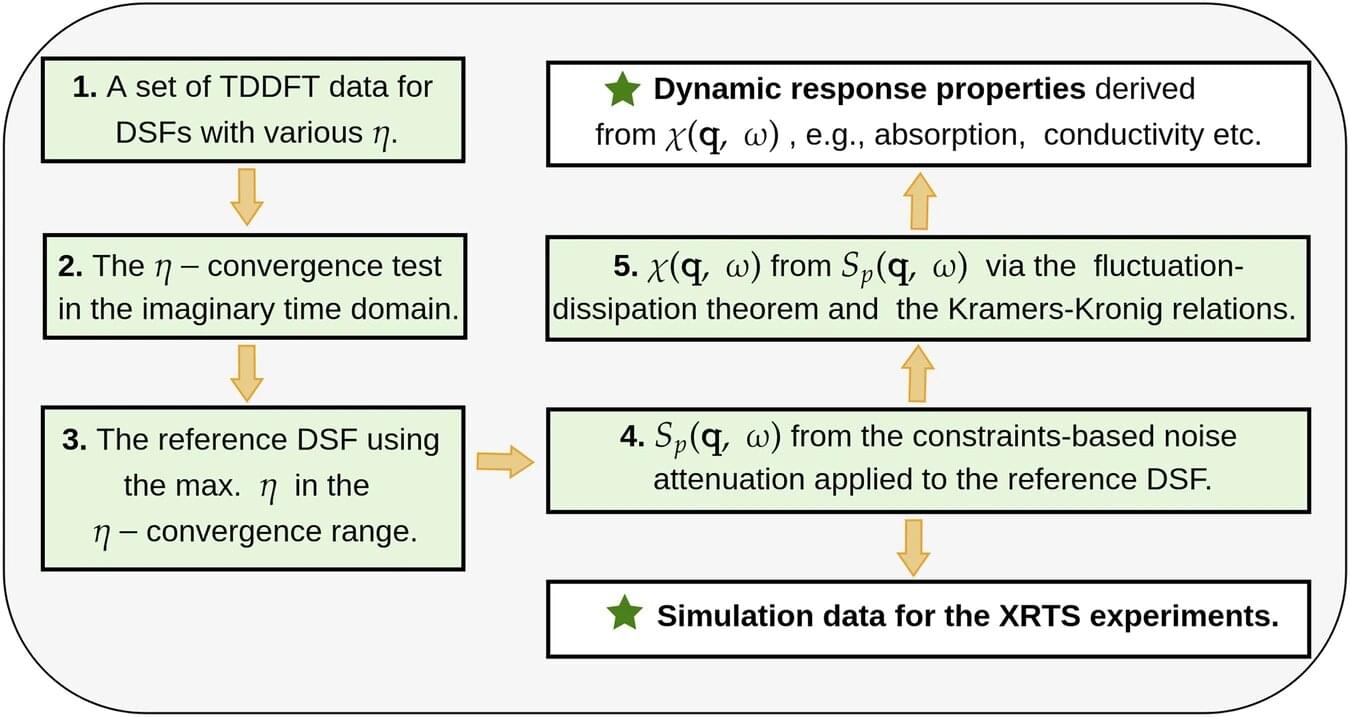
Researchers at the Helmholtz-Zentrum Dresden-Rossendorf (HZDR) have developed a new procedure, enabling them to speed up elaborate computer simulations that analyze matter under extreme conditions. In particular, this work improves the evaluation of experiments at large-scale research facilities like the European XFEL—and should facilitate substantial progress, among others, in fusion research and laboratory astrophysics.
The team presented the results in the journal npj Computational Materials.
Sometimes, matter is present in extreme states—such as in stars or in the interior of gas giants where enormous pressures and temperatures prevail. Such conditions can also be produced in the lab, in laser fusion experiments, for instance. In order to understand precisely what happens, researchers use X-ray scattering—as at the European XFEL near Hamburg.

The modern world runs on invisible energy. Hidden inside smartphones, laptops, and electric vehicles, are batteries that quietly power everyday life. As society becomes increasingly dependent on portable and sustainable energy, the development of compact and reliable battery technology has become one of the most important technological challenges of our time.
Lithium-ion batteries currently dominate the battery industry, but alternatives that could offer improved safety, lower cost, and higher energy density are being actively explored. Solid-state magnesium batteries have long been considered a promising next-generation energy technology. However, instability inside these batteries remains a major obstacle to their development.
New research led by a graduating Ph.D. student in The University of New Mexico Department of Electrical and Computer Engineering has shown that randomization can improve quantum computer performance in the presence of noise.
Ph.D. student Leeseok Kim led the research under the advice of Assistant Professor Milad Marvian, with support from Changhao Yi, a former member of Marvian’s group. Their findings, titled “Faster Randomized Dynamical Decoupling,” are published in the journal Physical Review Letters and were presented at QSim 2025, an international conference in quantum simulation.
Quantum computers have the potential to solve certain problems faster than classical computers, with promising applications in areas such as simulation and discovery of new materials, optimization, and cryptography. However, building quantum computers that can solve practically relevant problems at scale remains difficult because they are susceptible to noise. Reducing noise more effectively is therefore a key challenge.

Anthropic appears to be preparing for the public rollout of “Mythos,” which was announced in April as a restricted model that poses major security risks to private and public software.
On April 7, Anthropic announced the Mythos in early preview and called it a new frontier model with strikingly advanced capabilities in computer security tasks.
Anthropic said the Mythos model shows major improvements in code reasoning and autonomy, far above its current flagship model, Opus 4.7.
