The fundamentals of quantum mechanics are minuscule. Scientists constantly home in on finer resolutions to measure, quantify, and control these fundamentals, like photons that carry light and have no mass unless they are moving. The more precise the measurement, the more possibilities for better quantum technology or the ability to detect elusive dark-matter axions in deep space.
Now, researchers in Finland have successfully used a calorimeter, a type of ultra-sensitive heat-based energy sensor, to detect energy levels below one zeptojoule, or a trillionth of a billionth of a joule. For context, a zeptojoule is approximately the amount of work it takes for a red blood cell to move a nanometer, or a billionth of a meter, upwards in Earth’s gravity.
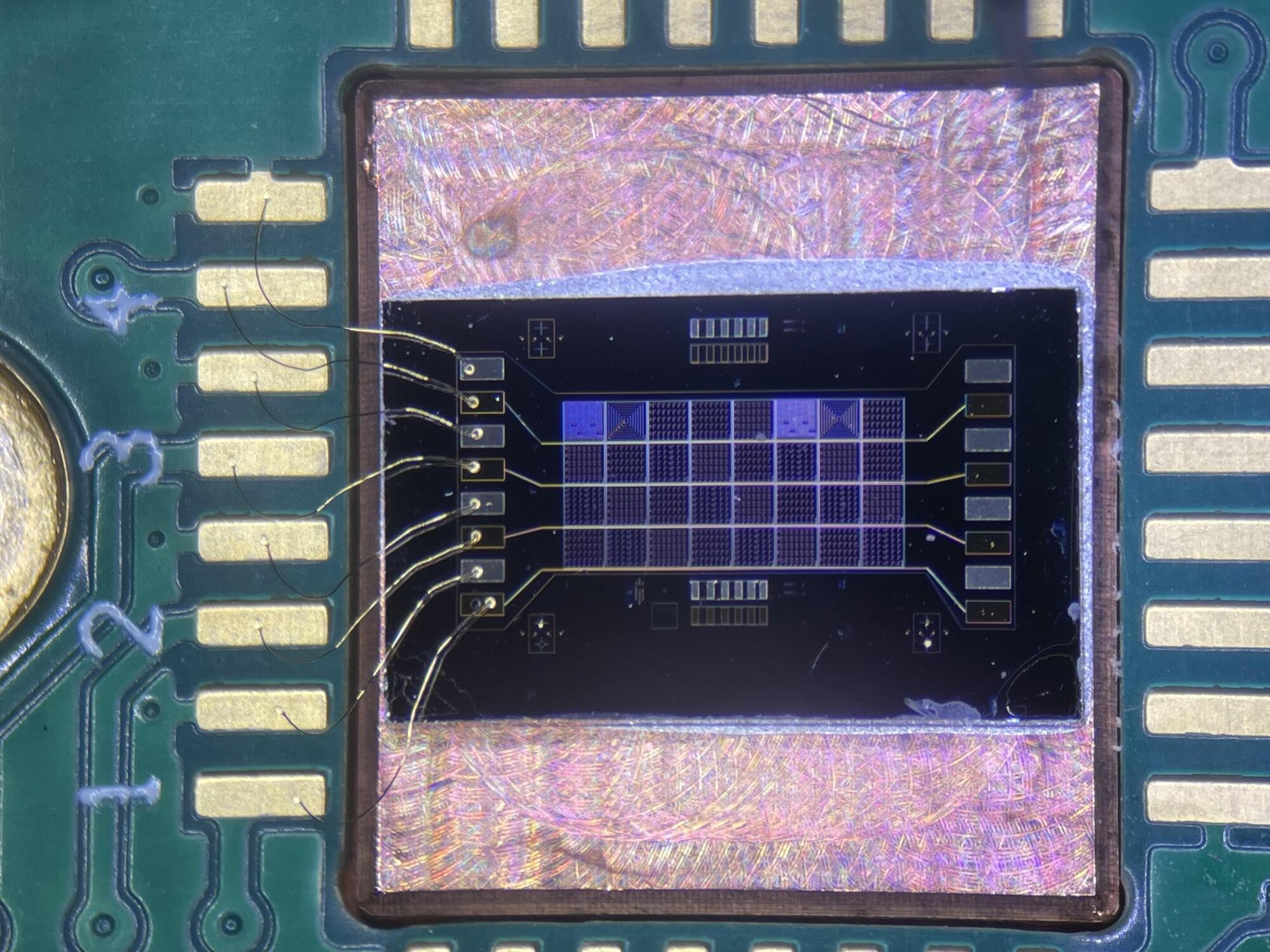
The team, led by Academy Professor Mikko Möttönen at Aalto University, together with industry collaborator IQM and the Technical Research Centre of Finland (VTT), used a novel technique to achieve the milestone measurement. The study is published in the journal Nature Electronics.