Toggle light / dark theme

Sustaining growth in storage and computational needs is increasingly challenging. For over a decade, exponentially more information has been produced year after year while data storage solutions are pressed to keep up. Soon, current solutions will be unable to match new information in need of storage. Computing is on a similar trajectory, with new needs emerging in search and other domains that require more efficient systems. Innovative methods are necessary to ensure the ability to address future demands, and DNA provides an opportunity at the molecular level for ultra-dense, durable, and sustainable solutions in these areas.

In this webinar, join Microsoft researcher Karin Strauss in exploring the role of biotechnology and synthetic DNA in reaching this goal. Although we have yet to achieve scalable, general-purpose molecular computation, there are areas of IT in which a molecular approach shows growing promise. These areas include storage as well as computation.

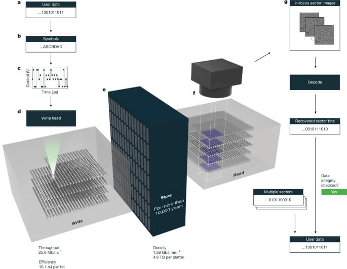
Learn how molecules, specifically synthetic DNA, can store digital data and perform certain types of special-purpose computation, like large-scale similarity search, by leveraging tools already developed by the biotechnology industry. Starting with some background on DNA and its storage potential, you’ll explore the advantages of using DNA for this application. Then, you’ll get a closer look at an end-to-end system, including encoding, synthesizing, reading, and decoding DNA. We’ll also look at an affordable full-stack digital microfluidics platform for wet lab preparations and conclude with a discussion of future hybrid systems.

Together, you’ll explore:

■ The intersection between technology and science of DNA data storage and computation.
■ The many advantages for using DNA to store data compared with other methods.
■ A detailed walkthrough of an end-to-end DNA storage system and its stages.
■ How DNA can be used for image similarity search.

In a new study, EPFL scientists visualized the intricate interplay between electron dynamics and solvent polarization in this process. This is a significant step in understanding a critical process of many chemical phenomena, and it might be the first step to improving energy conversion technologies.

CTTS is like a dance of microbes where one electron from a dissolved material (like salt) emerges and becomes part of the water. This produces a “hydrated” electron, essential for several watery processes, including those necessary for life. Comprehending CTTS is crucial to understanding the motion of electrons in solutions.

In a recent study, EPFL researchers Jinggang Lan, Majed Chergui, and Alfredo Pasquarello examined the complex interactions between electrons and their solvent surroundings. The work was mostly done at EPFL, with Jinggang Lan’s final contributions made while he was a postdoctoral fellow at the Simons Center for Computational Physical Chemistry at New York University.

Researchers at EPFL and the Max Planck Institute have incorporated nonlinear optical phenomena into a transmission electron microscope (TEM), which uses electrons for imaging instead of light.

- Advertisement -

Nonlinear optics, the study of unpredictable light behavior in materials, has applications in various fields, from laser development to quantum information science. Integrating nonlinear optics into a TEM enables complex light interactions on a small chip, allowing for the miniaturization of devices in applications such as optical signal processing, telecommunications, sensing, and spectroscopy.

Despite its success, FNP has some limitations: it can’t create stable particles larger than 400 nm, the maximum drug content is about 70 percent, the output is low, and it can only work with very hydrophobic (water-repelling) molecules. These issues arise because the particle core formation and particle stabilization happen simultaneously in FNP. The new SNaP process overcomes these limitations by separating the core formation and stabilization steps.

In the SNaP process, there are two mixing steps. First, the core components are mixed with water to start forming the particle core. Then, a stabilizing agent is added to stop the core growth and stabilize the particles. This second step must happen quickly, less than a few milliseconds after the first step, to control the particle size and prevent aggregation. Current SNaP setups connect two specialized mixers in series, controlling the delay time between steps. However, these setups face challenges, including high costs and difficulties in achieving short delay times needed for small particle formation.

A new approach using 3D printing has solved many of these challenges. Advances in 3D printing technology now allow the creation of precise, narrow channels needed for these mixers. The new design eliminates the need for external tubing between steps, allowing for shorter delay times and preventing leaks. The innovative stacked mixer design combines two mixers into a single setup, making the process more efficient and user-friendly.

The ultrafast dynamics and interactions of electrons in molecules and solids have long remained hidden from direct observation. For some time now, it has been possible to study these quantum-physical processes—for example, during chemical reactions, the conversion of sunlight into electricity in solar cells and elementary processes in quantum computers—in real time with a temporal resolution of a few femtoseconds (quadrillionths of a second) using two-dimensional electronic spectroscopy (2DES).

However, this technique is highly complex. Consequently, it has only been employed by a handful of research groups worldwide to date. Now a German-Italian team led by Prof. Dr. Christoph Lienau from the University of Oldenburg has discovered a way to significantly simplify the experimental implementation of this procedure. “We hope that 2DES will go from being a methodology for experts to a tool that can be widely used,” explains Lienau.

Two doctoral students from Lienau’s Ultrafast Nano-Optics research group, Daniel Timmer and Daniel Lünemann, played a key role in the discovery of the new method. The team has now published a paper in Optica describing the procedure.

Physicists at the University of Cologne have taken an important step forward in the pursuit of topological quantum computing by demonstrating the first-ever observation of Crossed Andreev Reflection (CAR) in topological insulator (TI) nanowires.

This finding, published under the title “Long-range crossed Andreev reflection in topological insulator nanowires proximitized by a superconductor” in Nature Physics, deepens our understanding of superconducting effects in these materials, which is essential for realizing robust quantum bits (qubits) based on Majorana zero-modes in the TI platform—a major goal of the Cluster of Excellence Matter and Light for Quantum Computing (ML4Q).

Quantum computing promises to revolutionize information processing, but current qubit technologies struggle with maintaining stability and error correction. One of the most promising approaches to overcoming these limitations is the use of topological superconductors, which can host special quantum states called Majorana zero-modes.

Scientists at the Okinawa Institute of Science and Technology (OIST), the National Institute of Information and Communications Technology, and the University of Tokyo have found a mathematical connection between spatial navigation and language processing, creating a model called “Disentangled Successor Information” (DSI).

This model generates patterns that closely resemble the activity of actual brain cells involved in both spatial awareness (place cells and grid cells) and concept recognition (concept cells).

The DSI model shows that the hippocampus and entorhinal cortex— previously known primarily for —likely use comparable computational processes to handle both physical spaces and meaningful ideas or words. Using this shared framework, both types of information can be processed through similar mathematical computations, which could be achieved in the brain by partial activation of specific groups of neurons.

Mind Control: Past and Future https://www.hks.harvard.edu/sites/default/files/2025-01/24_Meier_02.pdf


On Jan. 28, 2024, Noland Arbaugh became the first person to receive a brain chip implant from Neuralink, the neurotechnology company owned by Elon Musk. The implant seemed to work: Arbaugh, who is paralyzed, learned to control a computer mouse with his mind and even to play online chess.

The device is part of a class of therapeutics, (BCIs), that show promise for helping people with disabilities control prosthetic limbs, operate a computer, or translate their thoughts directly into speech. Current use of the technology is limited, but with millions of global cases of spinal cord injuries, strokes, and other conditions, some estimates put the market for BCIs at around $400 billion in the U.S. alone.

A new discussion paper from the Carr Center for Human Rights welcomes the potential benefits but offers a note of caution drawn from the past, detailing unsettling parallels between an era of new therapies and one of America’s darkest chapters: experiments into psychological manipulation and mind control.

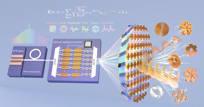
Researchers at the University of Twente, in collaboration with the City University of Hong Kong, have designed a cutting-edge programmable photonic chip in a thin-film lithium niobate platform, an important material in photonics. Published in Nature Communications, this work paves the way for next-generation high-performance radar and communication applications.

An important material is changing the way work, making them smaller, faster, and more efficient: thin-film lithium niobate (TFLN). It offers exceptional properties for how light and electrical signals can interact. This enables the seamless integration of key components—such as electro-optic modulators and signal processors—onto a single chip. As a result, can achieve unprecedented compactness, efficiency, and performance.

Researchers at the University of Twente have designed a TFLN-based integrated photonic chip, working in close collaboration with City University of Hong Kong, where the fabrication takes place. At the same time, these chips are also being fabricated locally in the MESA+ Nanolab.