Toggle light / dark theme

In a first, scientists observe short-range order in semiconductors

Inside the microchips powering your devices, atoms aren’t just randomly scattered. They follow a hidden order that can change how semiconductors behave.

A team of researchers from the Lawrence Berkeley National Laboratory (Berkeley Lab) and George Washington University has, for the first time, observed these tiny patterns, called short-range order (SRO), directly in semiconductors.

This discovery is a game-changer, as understanding how atoms naturally arrange themselves could let researchers design materials with desirable electronic properties. Such control could revolutionize quantum computing, neuromorphic devices that mimic the brain, and advanced optical detectors.

Thinking outside the box to fabricate customized 3D neural chips

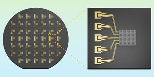
Cultured neural tissues have been widely used as a simplified experimental model for brain research. However, existing devices for growing and recording neural tissues, which are manufactured using semiconductor processes, have limitations in terms of shape modification and the implementation of three-dimensional (3D) structures.

By thinking outside the box, a KAIST research team has successfully created a customized 3D neural chip. They first used a 3D printer to fabricate a hollow channel structure, then used to automatically fill the channels with conductive ink, creating the electrodes and wiring. This achievement is expected to significantly increase the design freedom and versatility of brain science and brain engineering research platforms. The paper is published in the journal Advanced Functional Materials.

A research team led by Professor Yoonkey Nam from the Department of Bio and Brain Engineering has successfully developed a platform technology that overcomes the limitations of traditional semiconductor-based manufacturing. This technology allows for the precise fabrication of a 3D microelectrode array (neural interfaces with multiple microelectrodes arranged in a 3D space to measure and stimulate the electrophysiological signal of neurons) in various customized forms for in vitro culture chips.

Wade Demmer — VP, R&D, Medtronic — The Future Of Pacemaker Technologies

The future of pacemaker technologies — wade demmer — VP, R&D, medtronic.


Wade Demmer is Vice President of Research & Development at Medtronic where he is responsible for the development of new generations of pacemakers (https://www.medtronic.com/en-us/l/patients/treatments-therap…ers.html). With extensive expertise in medical technology and innovation, he leads the company’s R&D efforts to develop cutting-edge healthcare solutions and is dedicated to advancing medical advancements that improve patient outcomes and transform healthcare delivery.

Wade began his career at Intel, where he gained valuable experience in technology development and engineering. Building on his technical expertise, he transitioned into the medical device industry, bringing a strong innovation-driven mindset to healthcare solutions.

Wade is best known for his pioneering work on pacemakers, where he contributed to the design and development of advanced cardiac pacing technologies. His innovative approaches have helped improve the reliability, longevity, and patient comfort of pacemaker devices, significantly impacting the field of cardiac care.

Wade received his Bachelor of Engineering (BEng), with a focus on Computer Engineering, from Iowa State University, and his MBA from University of Minnesota Carlson School of Management.

$793M Economic Impact: SEALSQ to Launch Spain’s First Post-Quantum Semiconductor Center with Quantix

SEALSQ partners with Quantix Edge Security on €19.6M government-backed quantum chip facility in Murcia, Spain. Project starts H1 2026, includes QS7001 chip launch in November 2025.

Compact camera uses 25 color channels for high-speed, high-definition hyperspectral video

A traditional digital camera splits an image into three channels—red, green and blue—mirroring how the human eye perceives color. But those are just three discrete points along a continuous spectrum of wavelengths. Specialized “spectral” cameras go further by sequentially capturing dozens, or even hundreds, of these divisions across the spectrum.

This process is slow, however, meaning that hyperspectral cameras can only take still images, or videos with very low frame rates, or frames per second (fps). But what if a high-fps video camera could capture dozens of wavelengths at once, revealing details invisible to the naked eye?

Now, researchers at the University of Utah’s John and Marcia Price College of Engineering have developed a new way of taking a high-definition snapshot that encodes spectral data into images, much like a traditional camera encodes color. Instead of a filter that divides light into three color channels, their specialized filter divides it into 25. Each pixel stores compressed spectral information along with its , which computer algorithms can later reconstruct into a “cube” of 25 separate images—each representing a distinct slice of the visible spectrum.

Atomic neighborhoods in semiconductors provide new avenue for designing microelectronics

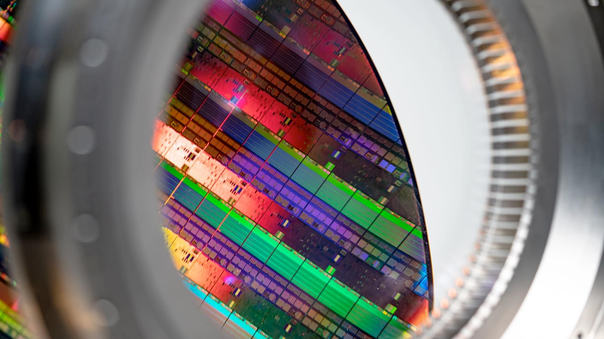
Inside the microchips powering the device you’re reading this on, the atoms have a hidden order all their own. A team led by Lawrence Berkeley National Laboratory (Berkeley Lab) and George Washington University has confirmed that atoms in semiconductors will arrange themselves in distinctive localized patterns that change the material’s electronic behavior.

The research, published in Science, may provide a foundation for designing specialized semiconductors for quantum-computing and optoelectronic devices for defense technologies.

On the , semiconductors are crystals made of different elements arranged in repeating . Many semiconductors are made primarily of one element with a few others added to the mix in small quantities. There aren’t enough of these trace additives to cause a throughout the material, but how these atoms are arranged next to their immediate neighbors has long been a mystery.

Chip-scale cold atom experiments could unleash the power of quantum science in the field

Cold atom experiments are among the most powerful and precise ways of investigating and measuring the universe and exploring the quantum world. By trapping atoms and exploiting their quantum properties, scientists can discover new states of matter, sense even the faintest of signals, take ultra-precise measurements of time and gravity, and conduct quantum sensing and computing experiments.

Quantum random number generator combines small size and high speed

Researchers have developed a chip-based quantum random number generator that provides high-speed, high-quality operation on a miniaturized platform. This advance could help move quantum random number generators closer to being built directly into everyday devices, where they could strengthen security without sacrificing speed.

Preserving particle physics data ensures future discoveries from collider experiments

A lot of the science from our accelerators is published long after collisions end, so storing experimental data for future physicists is crucial.

About a billion pairs of particles collide every second within the Large Hadron Collider (LHC). With them, a petabyte of collision data floods the detectors and pours through highly selective filters, known as trigger systems. Less than 0.001% of the data survives the process and reaches the CERN Data Center, to be copied onto long-term tape.

This archive now represents the largest scientific data set ever assembled. Yet, there may be more science in it than we can extract today, which makes data preservation essential for future physicists.

/* */