Toggle light / dark theme

New method realize ohmic contacts in n-type MoS₂ transistors at cryogenic temperatures

Semiconducting transition metal dichalcogenides (TMDs) are a class of layered materials exhibiting unique optoelectronic properties that could be leveraged to develop transistors, sensors and other nanoelectronics. Despite their advantages, creating robust ohmic contacts that connect a metal electrode in transistors to semiconducting TMDs at cryogenic temperatures has proved challenging.

This has so far limited the use of these materials for either studying or developing nanoelectronics that operate at low temperatures.

In a paper in Nature Electronics, researchers at the Liaoning Academy of Materials, Shanxi University and other institutes introduced a new technique for realizing ohmic contacts to the TMD molybdenum disulfide (MoS2) at , and found that in those transistors can be surprisingly high.

Earth’s atmosphere may help support human life on the moon

The moon’s surface may be more than just a dusty, barren landscape. Over billions of years, tiny particles from Earth’s atmosphere have landed in the lunar soil, creating a possible source of life-sustaining substances for future astronauts. But scientists have only recently begun to understand how these particles make the long journey from Earth to the moon and how long the process has been taking place.

New research from the University of Rochester, published in Communications Earth & Environment, shows that Earth’s magnetic field may actually help guide atmospheric particles—carried by solar wind—into space, instead of blocking them. Because Earth’s magnetic field has existed for billions of years, this process could have steadily moved particles from Earth to the moon over very long periods of time.

“By combining data from particles preserved in lunar soil with computational modeling of how solar wind interacts with Earth’s atmosphere, we can trace the history of Earth’s atmosphere and its magnetic field,” says Eric Blackman, a professor in the Department of Physics and Astronomy and a distinguished scientist at URochester’s Laboratory for Laser Energetics (LLE).

Chip-scale magnetometer uses light for high-precision magnetic sensing

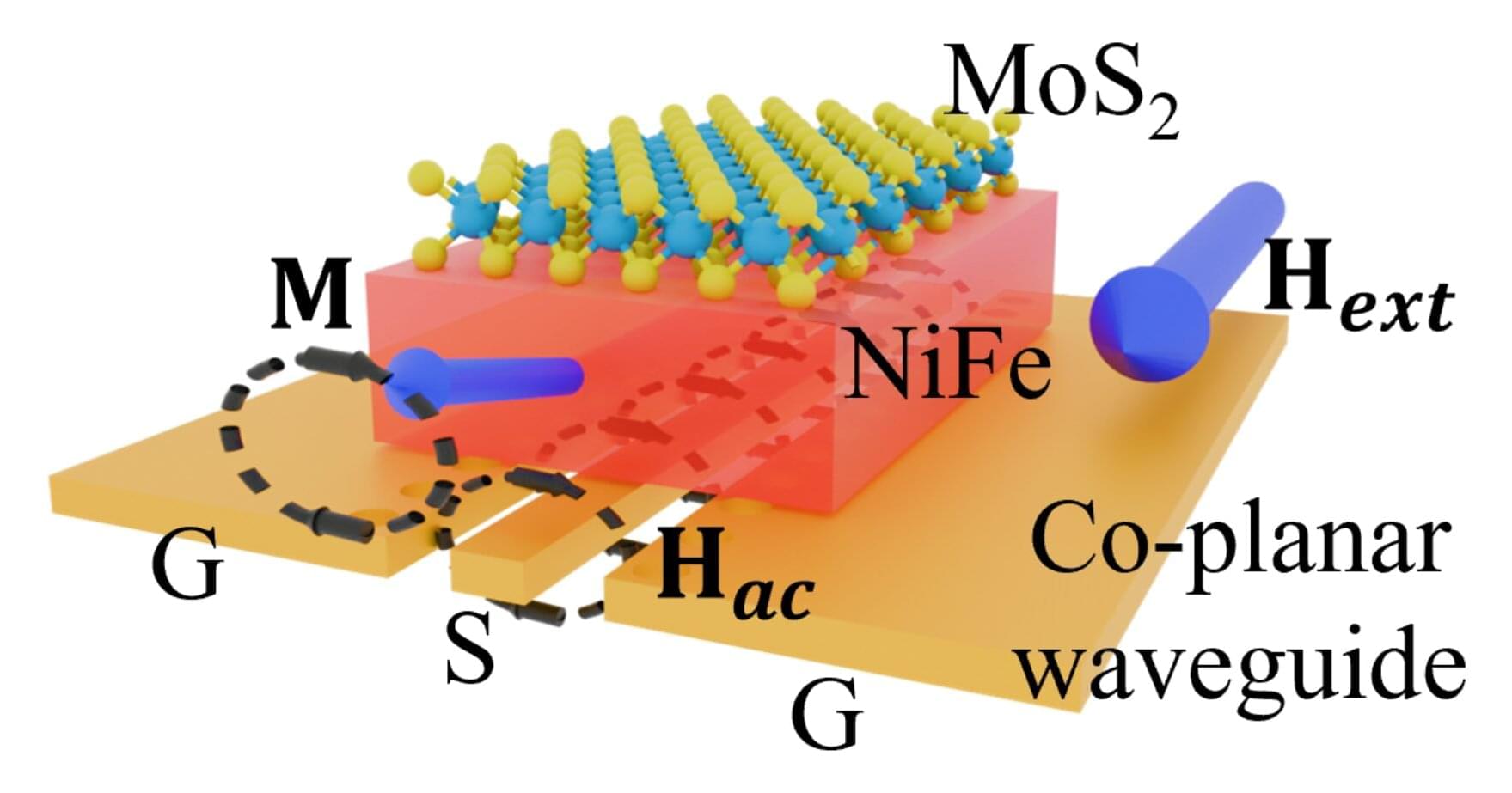
Researchers have developed a precision magnetometer based on a special material that changes optical properties in response to a magnetic field. The device, which is integrated onto a chip, could benefit space missions, navigation and biomedical applications.

High-precision magnetometers are used to measure the strength and direction of magnetic fields for various applications. However, many of today’s magnetometers must operate at extremely low temperatures—close to 0 kelvin—or require relatively large and heavy apparatus, which significantly restricts their practicality.

“Our device operates at room temperature and can be fully integrated onto a chip,” said Paolo Pintus from the University of California, Santa Barbara (UCSB) and the University of Cagliari, Italy, co-principal investigator for the study. “The light weight and low power consumption of this magnetometer make it ideal for use on small satellites, where it could enable studies of the magnetic areas around planets or aid in characterizing foreign metallic objects in space.”

Transistor ‘design limitation’ actually improves performance, scientists find

What many engineers once saw as a flaw in organic electronics could actually make these devices more stable and reliable, according to new research from the University of Surrey and Joanneum Research Materials.

The paper, which will be presented at the IEEE International Electron Devices Meeting (IEDM) 2025, describes how embracing small energy barriers at the metal/semiconductor interface of organic thin-film transistors (OTFTs) can help them perform more consistently and operate more reliably over time.

Organic thin-film transistors (OTFTs) are a key component of what are thought to be the next generation of flexible and wearable electronics. They are lightweight, low-cost and printable on large areas, but their long-term stability has been a persistent challenge.

Tiny optical modulator could enable giant future quantum computers

Researchers have made a major advance in quantum computing with a new device that is nearly 100 times smaller than the diameter of a human hair.

Published in the journal Nature Communications, the breakthrough optical phase modulators could help unlock much larger quantum computers by enabling efficient control of lasers required to operate thousands or even millions of qubits—the basic units of quantum information.

Critically, the team of scientists have developed these devices using scalable manufacturing, avoiding complex, custom builds in favor of those used to make the same technology behind processors already found in computers, phones, vehicles, home appliances—virtually everything powered by electricity (even toasters).

New materials could boost the energy efficiency of microelectronics

MIT researchers have developed a new fabrication method that could enable the production of more energy efficient electronics by stacking multiple functional components on top of one existing circuit.

In traditional circuits, logic devices that perform computation, like transistors, and memory devices that store data are built as separate components, forcing data to travel back and forth between them, which wastes energy.

This new electronics integration platform allows scientists to fabricate transistors and memory devices in one compact stack on a semiconductor chip. This eliminates much of that wasted energy while boosting the speed of computation.

New iron telluride thin film achieves superconductivity for quantum computer chips

If quantum computing is going to become an every-day reality, we need better superconducting thin films, the hardware that enables storage and processing of quantum information. Too often, these thin films have impurities or other defects that make them useless for real quantum computer chips.

Now, Yuki Sato and colleagues at the RIKEN Center for Emergent Matter Science (CEMS) in Japan have discovered a way to make a superconducting thin film from iron telluride, which is surprising because it is not normally superconducting.

The fabrication process reduces distortion in the crystal structure, making it superconducting at very low temperatures, and thus suitable for use in quantum chips. This study was published in Nature Communications.

Theoretical results could lead to faster, more secure quantum technology

University of Iowa researchers have discovered a method to “purify” photons, an advance that could make optical quantum technologies more efficient and more secure.

The work is published in the journal Optica Quantum.

The researchers investigated two nagging challenges to creating a steady stream of single photons, the gold standard method for realizing photonic quantum computers and secure communication networks. One obstacle is called laser scatter, which occurs when a laser beam is directed at an atom, causing it to emit a photon, which is a single unit of light. While effective, the technique can yield extra, redundant photons, which hampers the optical circuit’s efficiency, much like a wayward current in an electrical circuit.

/* */