Despite its success, FNP has some limitations: it can’t create stable particles larger than 400 nm, the maximum drug content is about 70 percent, the output is low, and it can only work with very hydrophobic (water-repelling) molecules. These issues arise because the particle core formation and particle stabilization happen simultaneously in FNP. The new SNaP process overcomes these limitations by separating the core formation and stabilization steps.
In the SNaP process, there are two mixing steps. First, the core components are mixed with water to start forming the particle core. Then, a stabilizing agent is added to stop the core growth and stabilize the particles. This second step must happen quickly, less than a few milliseconds after the first step, to control the particle size and prevent aggregation. Current SNaP setups connect two specialized mixers in series, controlling the delay time between steps. However, these setups face challenges, including high costs and difficulties in achieving short delay times needed for small particle formation.
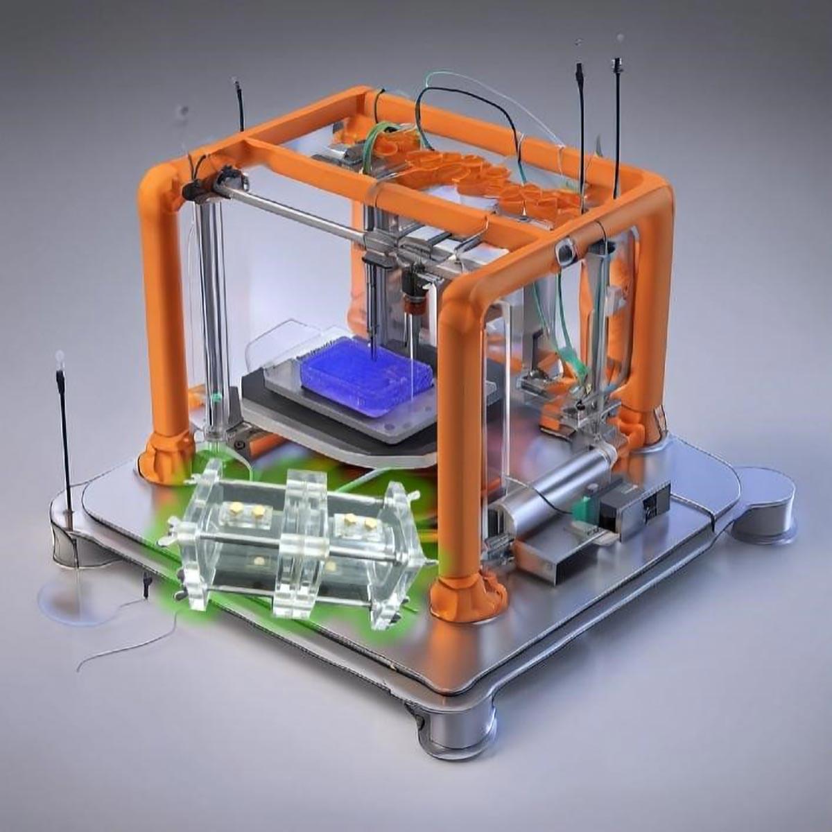
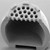
A new approach using 3D printing has solved many of these challenges. Advances in 3D printing technology now allow the creation of precise, narrow channels needed for these mixers. The new design eliminates the need for external tubing between steps, allowing for shorter delay times and preventing leaks. The innovative stacked mixer design combines two mixers into a single setup, making the process more efficient and user-friendly.