Menu

Blog

Page 5

Sep 8, 2024

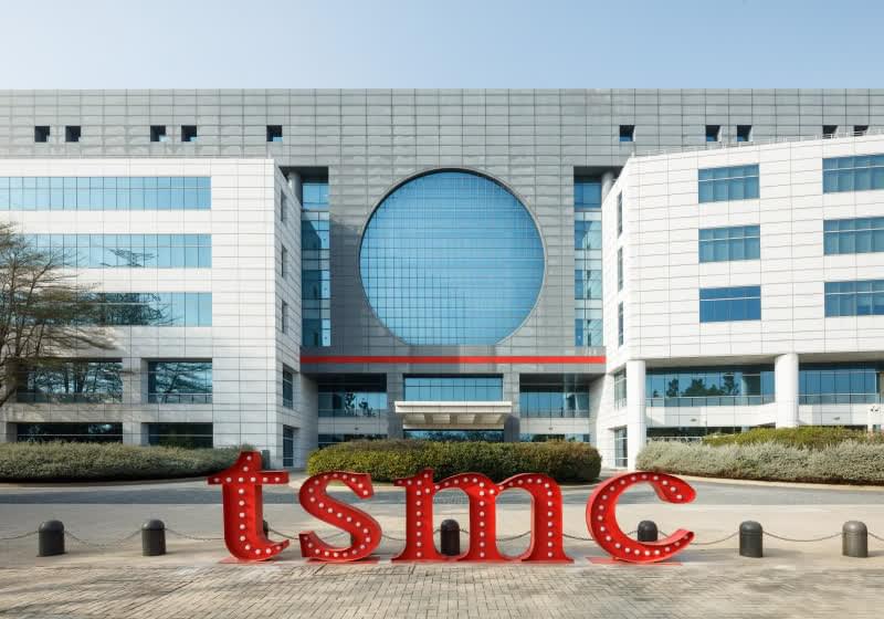
TSMC’s $65 billion Arizona facility can now match Taiwan production yields according to early trials

Posted by in categories: engineering, government

The big picture: The US is committed to establishing semiconductor manufacturing within its borders, and perhaps no effort is more crucial to this goal than TSMC’s three-fab facility in Arizona. The government is pouring billions into the development, alongside TSMC’s $65 billion investment.

Taiwan Semiconductor Manufacturing Co. has reached a significant milestone in its expansion into the US. Recent trial production at the company’s new Arizona facility has yielded results comparable to those of its established plants in Taiwan, according to Bloomberg, which cited a person familiar with the company who requested anonymity. This development is a positive sign for the chipmaker’s ambitious US project, which has faced delays and doubts about whether it could match the production efficiency of its Taiwanese operations.

The Arizona plant began engineering wafer production in April using advanced 4-nanometer process technology. With production yields now on par with its facilities in Tainan, Taiwan, TSMC should be able to maintain its targeted gross margin rates of 53 percent or higher.

Sep 8, 2024

Researchers develop approach to fabricate highly performing transistors based on 2D semiconductors

Posted by in categories: computing, materials

Two-dimensional (2D) semiconducting materials have distinct optoelectronic properties that could be advantageous for the development of ultra-thin and tunable electronic components. Despite their potential advantages over bulk semiconductors, optimally interfacing these materials with gate dielectrics has so far proved challenging, often resulting in interfacial traps that rapidly degrade the performance of transistors.

Researchers at King Abdullah University of Science and Technology (KAUST), Soochow University and other institutes worldwide recently introduced an approach that could enable the fabrication of better performing transistors based on 2D semiconductors. Their proposed design, outlined in a paper in Nature Electronics, entails the use of hexagonal boron nitride (h-BN) dielectrics and metal gate electrodes with a high cohesive energy.

“Initially, we found that when we use platinum (Pt) as an anode, the h-BN stack is less likely to trigger breakdown,” Yaqing Shen, first author of the paper, told Tech Xplore. “Based on this finding, we designed our experiments and found that Pt/h-BN gate stacks show 500-times lower leakage current than Au/h-BN gate stacks and exhibit a high dielectric strength of at least 25 MV/cm. This gave us the idea of using CVD h-BN as a gate dielectric in 2D transistors.”

Sep 8, 2024

Qualcomm CEO Reveals Smart Glasses Partnership With Google and Samsung

Posted by in category: mobile phones

Sep 7, 2024

Revolutionizing 3D printing through microwave technology

Posted by in categories: 3D printing, biotech/medical

In the rapidly evolving world of 3D printing, the pursuit of faster, more efficient and versatile production methods is never-ending. Traditional 3D printing techniques, while groundbreaking, are often time-consuming and limited in the kinds of materials they can use as feedstock.

But, through a new process a Lawrence Livermore National Laboratory (LLNL) team is calling Microwave Volumetric Additive Manufacturing (MVAM), researchers have introduced an innovative new approach to 3D printing using microwave energy to cure materials, opening the door to a broader range of materials than ever before.

In a recent paper published in Additive Manufacturing Letters, LLNL researchers describe the potential of microwave energy to penetrate a wider range of materials compared to light-based volumetric additive manufacturing (VAM).

Sep 7, 2024

Why are black holes stable against their own gravity?

Posted by in categories: cosmology, quantum physics

Neutron stars are timelike matter with a maximum mass of about 2.34 solar masses in quantum chromodynamics (the strong color force). Black holes are spacelike matter that have no maximum mass, but a minimum mass of 2.35 solar masses. Indeed, black holes have been identified with millions or billions of solar masses.

Sep 7, 2024

New quantum error correction method uses ‘many-hypercube codes’ while exhibiting beautiful geometry

Posted by in categories: computing, quantum physics

In work published in Science Advances, Hayato Goto from the RIKEN Center for Quantum Computing in Japan has proposed a new quantum error correction approach using what he calls “many-hypercube codes.”

Sep 7, 2024

Researchers create a one-dimensional gas out of light

Posted by in category: quantum physics

Physicists at the University of Bonn and the University of Kaiserslautern-Landau (RPTU) have created a one-dimensional gas out of light. This has enabled them to test theoretical predictions about the transition into this exotic state of matter for the first time. The method used in the experiment by the researchers could be used for examining quantum effects. The results have been published in Nature Physics.

Sep 7, 2024

Theoretical research establishes unified way to quantify vital quantum properties

Posted by in category: quantum physics

The foundation of nearly all quantum information applications—such as computation and communication—rely on the quantum properties of superposition and entanglement.

Sep 7, 2024

Improved method for phonon lasers ‘locks’ sound waves into a more stable and powerful state

Posted by in category: biotech/medical

Scientists have made a significant leap in developing lasers that use sound waves instead of light. These phonon lasers hold promise for advancements in medical imaging, deep-sea exploration, and other areas.

Sep 7, 2024

Unlocking the secrets of diamond: New insights into nitrogen-vacancy center formation

Posted by in categories: biological, computing, quantum physics

Research teams from Wuhan University and the China University of Geosciences (Wuhan) have revealed new insights into the formation mechanism of nitrogen-vacancies (NV) centers in type-Ib diamonds, a phenomenon critical to quantum sensing and computing advancements. Using a novel irradiation and annealing method, the teams demonstrated how controlled temperature and orientation can significantly increase the density and depth of NV centers, paving the way for new applications in biological imaging and quantum technologies.

Page 5 of 11,699First23456789Last