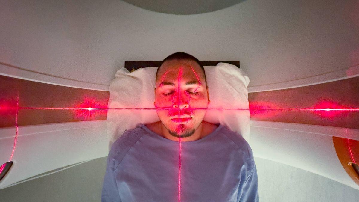
A new trial has come back with encouraging results
Get the latest international news and world events from around the world.
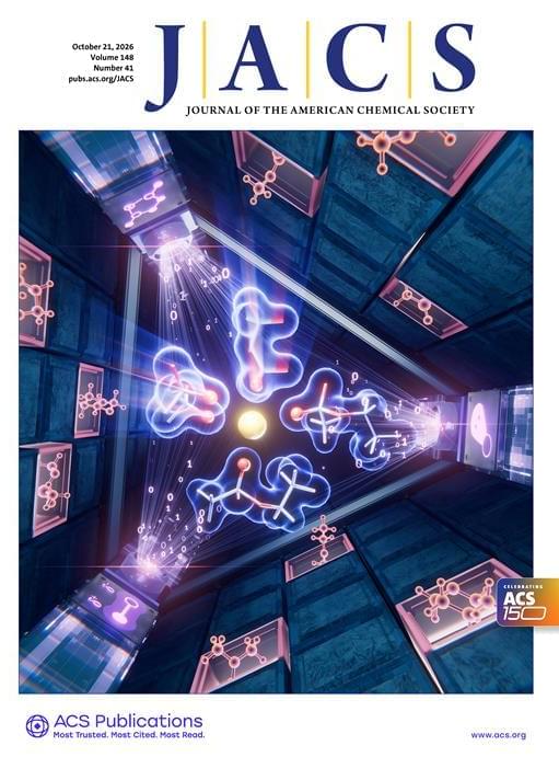
Enhanced Photocatalytic C–N Coupling by Synergistic Facet and Spin-State Modulation in Mixed-Valent WOx
This website uses a security service to protect against malicious bots. This page is displayed while the website verifies you are not a bot.
Consensus AI, 92 Longevity Podcasts Merged Into 1: Dave Pascoe Built It
Join us on Patreon! / michaellustgartenphd.
Discount Links/Affiliates:
Blood testing (where I get the majority of my labs, for those who blood test with Quest): https://www.ultalabtests.com/partners… those who blood test with LabCorp: https://www.anrdoezrs.net/click-10161… At-Home Metabolomics: https://www.iollo.com?ref=michael-lus… Use Code: CONQUERAGING At Checkout Clearly Filtered Water Filter: https://get.aspr.app/SHoPY Epigenetic, Telomere Testing: https://trudiagnostic.com/?irclickid=… Use Code: CONQUERAGING NAD+ Quantification: https://www.jinfiniti.com/intracellul… Use Code: ConquerAging At Checkout Oral Microbiome: https://www.bristlehealth.com/?ref=mi… Enter Code: ConquerAging SiphoxHealth Blood Testing (ApoB, GrimAge): https://siphoxhealth.com/mlustgarten Green Tea: https://www.ochaandco.com/?ref=fqbtflod Use Code: ML10OFF Diet Tracking: https://shareasale.com/r.cfm?b=139013… If you’d like to support the channel, you can do that with the website, Buy Me A Coffee: https://www.buymeacoffee.com/mlhnrca Conquer Aging Or Die Trying Merch! https://my-store-d4e7df.creator-sprin…
Blood Testing Essentials (Biological Age, CVD-Risk, Kidney Health and Function):
PhenoAge (Biological Age): https://www.ultalabtests.com/partners…
Measure the Bortz biological clock biomarkers: https://www.ultalabtests.com/partners…
Calculate your biological age using the Bortz clock: https://www.longevity-tools.com/human…
AGE TRIAL RESULTS!!! + A Drink Designed By AI to Reverses Aging
The first age reversal gene therapy ever given to people just reported results. Life Biosciences’ ER-100, co-founded by Harvard’s David Sinclair, uses three Yamanaka factors (OSK) to try to reset aging cells in the eye. In the first three glaucoma patients, the low dose was well tolerated and two of the three improved on visual field testing. We break down how it works, where the viral \.
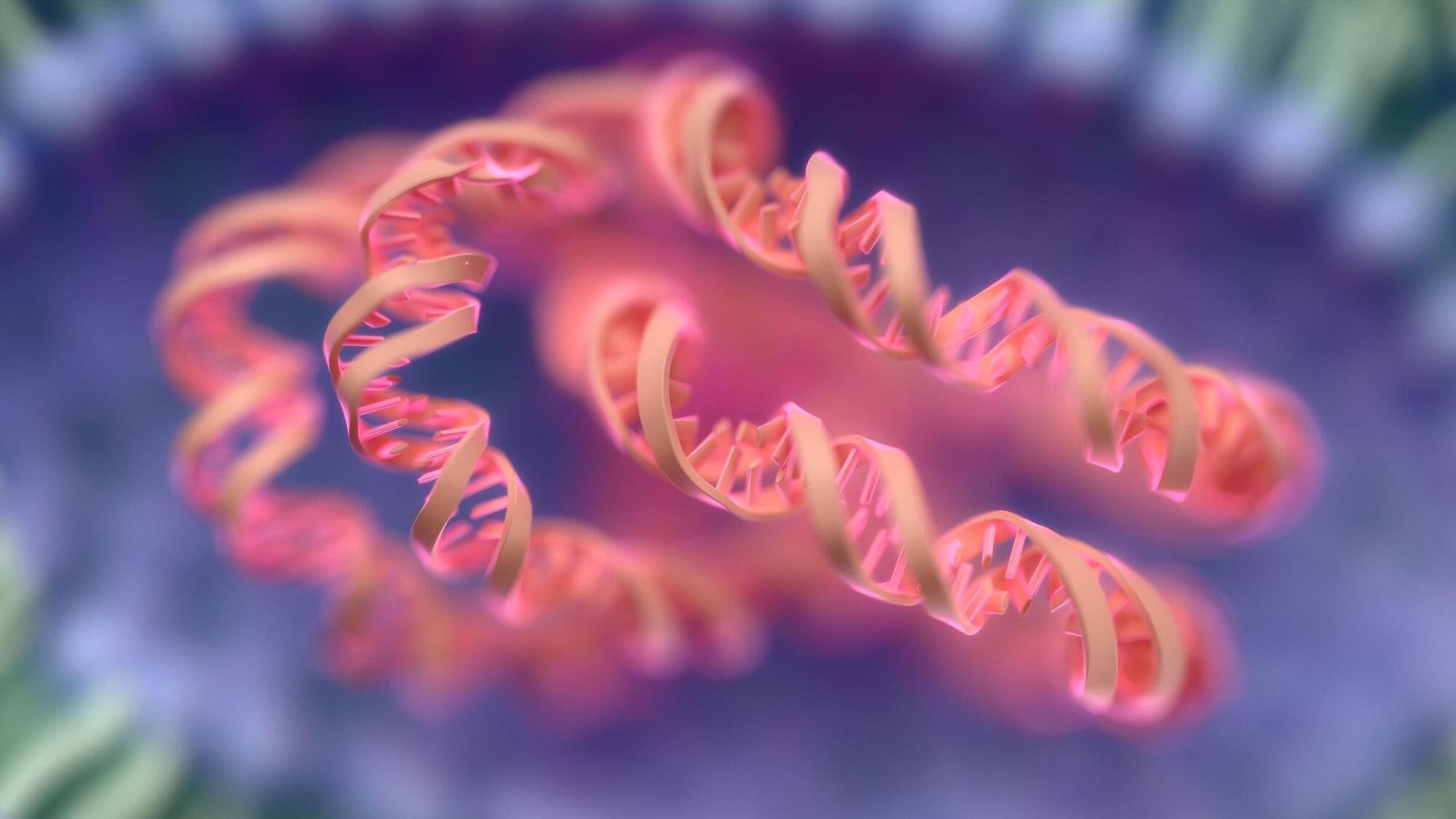
Too Much RNA Can Actually Starve Cells of Energy, Study Finds
RNA, or ribonucleic acid, is one of the most important molecules in keeping the body functioning correctly. One of its main jobs is to turn the information stored in our genetics into actual proteins that build and operate cells, for example.
To stay healthy, cells keep RNA production and deletion in a careful balance, but there are ways this balance can be tipped over. Invading viruses tend to produce more RNA, and aging, certain cancers, and neurodegenerative diseases can also cause disruption.
In a study published in PNAS, researchers outline a newly discovered way that too much RNA can cause harm: It can interfere with tiny power plants called mitochondria inside cells, limiting their energy production capacities.

Could Drugs for Diabetes and ADHD Offer New Hope for Alzheimer’s Patients?
The AD-SMART trial will initially test two repurposed medicines. One is metformin, widely used to treat type 2 diabetes. The other is atomoxetine, a drug prescribed for attention deficit hyperactivity disorder, or ADHD. An international expert panel selected these drugs based on early evidence that they may reduce brain inflammation, which scientists believe is one of the drivers of neurodegeneration in Alzheimer’s disease.
Professor Paresh Malhotra, chief investigator of the study and group leader at the UK Dementia Research Institute Centre for Care Research & Technology at Imperial College London, described a central problem in Alzheimer’s research. He noted that for too long progress has followed a pattern of one drug, one trial, one answer, often taking a decade or more for each attempt. AD-SMART is a deliberate effort to break this pattern and accelerate the path to answers for patients and families.
The design of the trial is particularly notable. AD-SMART is a multi-arm, multi-stage platform trial. Instead of testing a single drug against a placebo over many years, it evaluates several treatments at the same time against one shared placebo group. People who join the study have a higher chance of receiving an active treatment compared with many traditional trials, where a large proportion of participants might receive a placebo alone.

GLP-1s Rank Highly in New Framework for Anti-Aging Drug Development
A theoretical model proposes evaluating aging therapies by their potential to restore function safely rather than relying only on aging biomarkers. The approach offers testable predictions but needs experimental and clinical validation.

Revisiting post-stimulus theta activity: evidence for a broadband rather than narrowband spectral origin
The aperiodic, 1/f-like component of electrophysiological activity is increasingly recognized as a meaningful feature of neural function rather than background noise. Meanwhile, many EEG studies interpret transient post-stimulus changes in oscillatory power as signatures of attention, salience, or cognitive control. Such interpretations typically depend on baseline normalization, which assumes aperiodic activity remains stable from pre-to post-stimulus periods. Using high-density EEG from typically developing children, we tested this assumption across two paradigms: an audiovisual simple reaction-time task (n = 36, 19 males and 17 females) and a visual oddball task (n = 38, 20 males and 18 females). In each, conventional spectral analyses were compared with analyses that explicitly modeled and removed aperiodic activity in both windows. Across tasks, stimulus onset produced robust increases in aperiodic exponent and offset, indicating systematic 1/f changes. In the audiovisual task these were modality-specific, with central, parieto-occipital, or combined topographies by stimulus type. They diminished but persisted after ERP removal, suggesting they were not fully explained by phase-locked activity. Critically, once aperiodic activity was accounted for, the apparent theta increase was largely abolished in both tasks, including the canonical fronto-central enhancement to infrequent targets. The conventional method also overestimated beta desynchronization, especially in the induced signal, indicating a spurious consequence of spectral slope steepening. By contrast, alpha desynchronization remained robust and was enhanced, reflecting genuine suppression. Together, these findings suggest many conventional time-frequency effects, particularly apparent theta synchronization, may reflect stimulus-driven aperiodic changes rather than robust narrowband changes, challenging core assumptions of these analyses.
Significance statement Frequency-domain neural activity comprises both narrowband oscillations and broadband aperiodic activity. Conventional time–frequency analyses use baseline normalization to isolate oscillatory responses, implicitly assuming that aperiodic activity remains stable following stimulus onset. Across two EEG paradigms, we show that stimulus presentation systematically alters aperiodic activity in a sensory-and attention-dependent manner. These changes can produce apparent increases in theta-band power that do not reflect genuine narrowband oscillations and can exaggerate beta desynchronization. In contrast, alpha desynchronization remained robust after accounting for aperiodic activity. These findings demonstrate that stimulus-related aperiodic changes can substantially influence conventional time–frequency measures and should be explicitly considered when interpreting post-stimulus oscillatory responses.
You Could Unlock Deeper Parts of Reality by Linking Your Mind With This Futuristic Device, Scientists Believe
This could finally unravel one of the hardest problems in science.

‘Stupendously large black holes’ aren’t a major component of dark matter, study finds
We still don’t know what dark matter is.