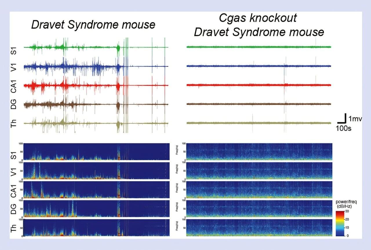
An overactive immune response in the brain may play a role in Dravet syndrome, a rare and severe genetic epilepsy that typically begins in infancy, according to Weill Cornell Medicine researchers. Children with the condition experience frequent seizures that are often difficult to control with medication and may also face developmental, cognitive and behavioral challenges. Until now, most research has focused on how a mutation in the SCN1A gene disrupts electrical signaling in the brain.
“Rather than being a disorder only involving abnormal electrical signaling, the disease may also involve a self-sustaining immune response triggered by DNA released from stressed neurons,” said study senior author Dr. Li Gan, the Burton P. and Judith B. Resnick Distinguished Professor in Neurodegenerative Diseases and director of the Helen and Robert Appel Alzheimer’s Disease Research Institute at Weill Cornell. “As a result, inflammation may help drive and sustain the disease. This finding links seizures to the brain’s immune system in a way that had not been fully appreciated before.”
The new preclinical study, published July 29 in Nature Neuroscience, identified an inflammatory pathway called cGAS-STING-interferon (IFN-I) signaling as a major contributor to disease progression. Blocking this molecular pathway could lead to new therapeutic strategies for epilepsy disorders.


