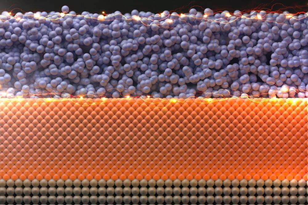
Toggle light / dark theme

Transparent and flexible displays, which have received a lot of attention in various fields including automobile displays, bio–health care, military, and fashion, are in fact known to break easily when experiencing small deformations. To solve this problem, active research is being conducted on many transparent and flexible conductive materials such as carbon nanotubes, graphene, silver nanowires, and conductive polymers.

A joint research team led by Professor Kyung Cheol Choi from the KAIST School of Electrical Engineering and Dr. Yonghee Lee from the National Nano Fab Center (NNFC) announced the successful development of a water-resistant, transparent, and flexible OLED using MXene nanotechnology. The material can emit and transmit light even when exposed to water.

This research was published as a front cover story of ACS Nano under the title “Highly Air-Stable, Flexible, and Water-Resistive 2D Titanium Carbide MXene-Based RGB Organic Light-Emitting Diode Displays for Transparent Free-Form Electronics.”

Researchers have created a quantum superposition state in a semiconductor nanostructure that might serve as a basis for quantum computing. The trick: two optical laser pulses that act as a single terahertz laser pulse.

A German-Chinese research team has successfully created a quantum bit in a semiconductor nanostructure. Using a special energy transition, the researchers created a state in a quantum dot—a tiny area of the semiconductor—in which an electron hole simultaneously possessed two different energy levels. Such superposition states are fundamental for quantum computing.

However, excitation of the state would require a large-scale free-electron that can emit light in the terahertz range. Additionally, this wavelength is too long to focus the beam on the tiny quantum dot. The German-Chinese team has now achieved the excitation with two finely tuned short-wavelength optical .

Many diseases can be successfully treated in the simple environment of a cell culture dish, but to successfully treat real people, the drug agent has to take a journey through the infinitely more complex environment within our bodies and arrive, intact, inside the affected cells. This process, called drug delivery, is one of the most significant barriers in medicine.

A collaboration between Lawrence Berkeley National Laboratory (Berkeley Lab) and Genentech, a member of the Roche Group, is working to break through some of the bottlenecks by designing the most effective lipid nanoparticles (LNPs)—tiny spherical pouches made of fatty molecules that encapsulate therapeutic agents until they dock with cell membranes and release their contents. The first drug to use LNPs was approved in 2018, but the delivery method rose to global prominence with the Pfizer and Moderna mRNA COVID vaccines.

“It’s quite a smart system, because if you just deliver the RNA itself to the human body, the RNA is degraded by nucleases and cannot easily cross the cell membrane due to its size and charge, but the LNPs deliver it safely into the cell,” explained co-lead author Chun-Wan Yen, a senior Principal Scientist in Genentech’s Small Molecule Pharmaceutical Sciences group.

A team of ingenious bioengineers at Arizona State University (ASU) has harnessed the power of childhood nostalgia, unveiling a creative solution to a long-standing challenge in DNA origami research.

They’ve successfully employed a LEGO robotics kit to build an affordable, highly effective gradient mixer for purifying self-assembling DNA origami nanostructures. This innovative breakthrough, detailed in a paper published one PLOS ONE, promises to revolutionize how scientists approach DNA origami synthesis.

The creation of DNA origami structures is an intricate process, requiring precise purification of nanostructures. Traditionally, this purification step involved rate-zone centrifugation, relying on a costly piece of equipment called a gradient mixer. However, the maverick minds at ASU have demonstrated that even the iconic plastic bricks of LEGO can be repurposed for scientific advancement.

Imagine shrinking light down to the size of a tiny water molecule, unlocking a world of quantum possibilities. This has been a long-held dream in the realms of light science and technology. Recent advancements have brought us closer to achieving this incredible feat, as researchers from Zhejiang University have made groundbreaking progress in confining light to subnanometer scales.

Traditionally, there have been two approaches to localize light beyond its typical diffraction limit: dielectric confinement and plasmonic confinement. However, challenges such as precision fabrication and optical loss have hindered the confinement of optical fields to sub-10 nanometer (nm) or even 1-nm levels. But now, a new waveguiding scheme reported in Advanced Photonics promises to unlock the potential of subnanometer optical fields.

Picture this: Light travels from a regular , embarking on a transformative journey through a fiber taper, and finds its destination in a coupled-nanowire-pair (CNP). Within the CNP, the light morphs into a remarkable nano-slit mode, generating a confined optical field that can be as tiny as a mere fraction of a nanometer (approximately 0.3 nm). With an astonishing efficiency of up to 95% and a high peak-to-background ratio, this novel approach offers a whole new world of possibilities.

Metals aren’t known to “heal” themselves on their own; once they break, it’s assumed the materials remain broken unless outside forces reform them. But new research into metallic properties indicates this isn’t always the case. In fact, some metals appear to naturally mend of their own accord—a discovery that could one day change engineering designs here on Earth and beyond.

According to a study published last week in Nature, materials scientists from Sandia National Laboratories in Albuquerque, New Mexico, and Texas A&M University discovered at least some metals—in this case copper and platinum—can “undergo intrinsic self-healing.” As Live Science recently noted, the team’s observations came completely by accident while observing the two materials at a nanoscale level.

[Related: Watch this metallic material move like the T-1000 from ‘Terminator 2’].

The interaction of light and matter on the nanoscale is a vital aspect of nanophotonics. Resonant nanosystems allow scientists to control and enhance electromagnetic energy at volumes smaller than the wavelength of the incident light. As well as allowing sunlight to be captured much more effectively, they also facilitate improved optical wave-guiding and emissions control. The strong coupling of light with electronic excitation in solid-state materials generates hybridized photonic and electronic states, so-called polaritons, which can exhibit interesting properties such as Bose-Einstein condensation and superfluidity.

Halide perovskites are a family of materials that have attracted attention for their superior optoelectronic properties and potential applications in devices such as high-performance solar cells, light-emitting diodes, and lasers.


Caption :

A new MIT platform enables researchers to “grow” halide perovskite nanocrystals with precise control over the location and size of each individual crystal, integrating them into nanoscale light-emitting diodes. Pictured is a rendering of a nanocrystal array emitting light.

Credit: Hyundai Motor Group.

During a press conference held yesterday in Seoul, South Korea, Hyundai Motor Group revealed plans for a new generation of high-tech cars incorporating nanoscale features, which it hopes to begin mass producing by 2025–2026.

Nanotechnology is defined as materials or devices that work on a scale smaller than one hundred nanometres (nm). A nanometre is one billionth of a metre or about 100,000 times narrower than a human hair. Individual atoms, for comparison, tend to range in size from 0.1 to 0.5 nm. Many interesting and unique physical effects become possible at this level of detail, making nanotechnology a highly promising technology of the future.

According to scientists at the U.S. Department of Energy’s National Renewable Energy Laboratory (NREL), a bifacial perovskite solar cell holds the potential to produce higher energy yields at lower overall costs.

The bifacial solar cell captures direct sunlight on the front and reflected sunlight on the back. As a result, this type of device can outperform its monofacial counterparts, according to the new study.

“This perovskite cell can operate very effectively from either side,” said Kai Zhu, a senior scientist in the Chemistry and Nanoscience Center at NREL and lead author of a new paper.