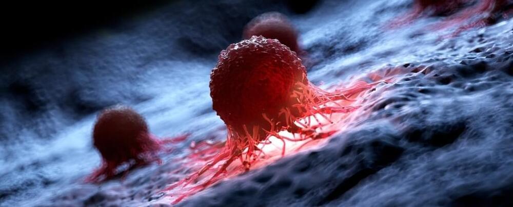
Year 2021 đđ
Nano Diamond Battery wants to bring its ânuclear-powered batteriesâ to the market within five years.
Year 2021 đđ
Nano Diamond Battery wants to bring its ânuclear-powered batteriesâ to the market within five years.
Engineers have been trying to devise increasingly efficient and low-cost methods to fabricate electronic components and devices on a large-scale. Recently, some studies explored the possibilities of creating electronics using solution processing techniques, which involve the deposition of materials with electrical properties from a solution onto a surface.
Researchers at Yonsei University and Sungkyunkwan University in South Korea recently fabricated wafer-scale transistor arrays based on the inorganic compound molybdenum-disulfide using a solution processing method. Their paper, published in Nature Electronics, could contribute to enabling the large-scale and low-cost fabrication of next-generation electronics.
âWe have been working on solution-processed 2D nanomaterials for scalable electronic applications for years, yet satisfying both electronic performance and scalability based on solution-based approaches has been very challenging until now,â Joonhoon Kang and Jeong Ho Cho, co-authors of the paper, told Tech Xplore.
Large area metalenses are on the horizon.
In this section, we briefly discuss the presented technique of VSB/CP e-beam writing in comparison with two other contemporary high-resolution lithographic patterning approaches: multibeam e-beam lithography, also known as complementary electron beam lithography (CEBL),16 and optical lithography.
Todayâs optical lithography tools are basically well able to address the feature-sizes of the elements presented in the previous section. The exposure in those tools is based on a demagnified imaging of a pattern containing photomask. With this parallel approach, optical lithography is always much faster than any direct-write technique. The central question for making a choice between optical lithography or VSB/CP-based e-beam lithography is, therefore, the effort needed to achieve the required optical performance. For the optical lithography, this is related to the quality of the mask. A high-resolution optical pattern may require a very fine approximation of the mask pattern, leading to large writing times in a mask shop and thus to considerable costs. Consequently, the choice between the different techniques must include considerations on the number of elements required and the price for which the final consumer product can be sold. This cannot be generalized.
The rapid development of wearable electronics requires its energy supply part to be flexible, wearable, integratable and sustainable. However, some of the energy supply units cannot meet these requirements at the same time, and there is also a capacity limitation of the energy storage units, and the development of sustainable wearable self-charging power supplies is crucial. Here, we report a wearable sustainable energy harvesting-storage hybrid self-charging power textile. The power textile consists of a coaxial fiber-shaped polylactic acid/reduced graphene oxide/polypyrrole (PLA-rGO-PPy) triboelectric nanogenerator (fiber-TENG) that can harvest low-frequency and irregular energy during human motion as a power generation unit, and a novel coaxial fiber-shaped supercapacitor (fiber-SC) prepared by functionalized loading of a wet-spinning graphene oxide fiber as an energy storage unit. The fiber-TENG is flexible, knittable, wearable and adaptable for integration with various portable electronics. The coaxial fiber-SC has high volumetric energy density and good cycling stability. The fiber-TENG and fiber-SC are flexible yarn structures for wearable continuous human movement energy harvesting and storage as on-body self-charging power systems, with light-weight, ease of preparation, great portability and wide applicability. The integrated power textile can provide an efficient route for sustainable working of wearable electronics.
Water and carbon make a quantum couple: the flow of water on a carbon surface is governed by an unusual phenomenon dubbed quantum friction. A new work published in Nature Nanotechnology experimentally demonstrates this phenomenonâwhich was predicted in a previous theoretical studyâat the interface between liquid water and graphene, a single layer of carbon atoms. Advanced ultrafast techniques were used to perform this study. These results could lead to applications in water purification and desalination processes and maybe even to liquid-based computers.
For the last 20 years, scientists have been puzzled by how water behaves near carbon surfaces. It may flow much faster than expected from conventional flow theories or form strange arrangements such as square ice. Now, an international team of researchers from the Max Plank Institute for Polymer Research of Mainz (Germany), the Catalan Institute of Nanoscience and Nanotechnology (ICN2, Spain), and the University of Manchester (England), reports in the study published in Nature Nanotechnology on June 22, 2023, that water can interact directly with the carbonâs electronsâa quantum phenomenon that is very unusual in fluid dynamics.
A liquid, such as water, is made up of small molecules that randomly move and constantly collide with each other. A solid, in contrast, is made of neatly arranged atoms that bathe in a cloud of electrons. The solid and the liquid worlds are assumed to interact only through collisions of the liquid molecules with the solidâs atomsâthe liquid molecules do not âseeâ the solidâs electrons. Nevertheless, just over a year ago, a paradigm-shifting theoretical study proposed that at the water-carbon interface, the liquidâs molecules and the solidâs electrons push and pull on each other, slowing down the liquid flow: this new effect was called quantum friction. However, the theoretical proposal lacked experimental verification.
Low-cost, flexible displays that use very little energy could be a step closer, thanks to an innovation from the University of Surrey that solves a problem that has plagued source-gated transistors (SGT). The study has been published by IEEE Transactions on Electron Devices.
Dr. Radu Sporea, project lead from the University of Surrey, said, We used a rapidly emerging semiconductor material called IGZO or indium-gallium-zinc oxide to create the next generation of source-gated transistors. Through nanoscale contact engineering, we obtained transistors that are much more stable with temperature than previous attempts. Device simulations allowed us to understand this effect.
This new design adds temperature stability to SGTs and retains usual benefits like using low power, producing high signal amplification, and being more reliable under different conditions. While source-gated transistors are not mainstream because of a handful of performance limitations, we are steadily chipping away at their shortcomings.
Aleksandra Radenovic, head of the Laboratory of Nanoscale Biology in the School of Engineering, has worked for years to improve nanopore technology, which involves passing a molecule like DNA through a tiny pore in a membrane to measure an ionic current. Scientists can determine DNAâs sequence of nucleotidesâwhich encodes genetic informationâby analyzing how each one perturbs this current as it passes through. The research has been published in Nature Nanotechnology.
Currently, the passage of molecules through a nanopore and the timing of their analysis are influenced by random physical forces, and the rapid movement of molecules makes achieving high analytical accuracy challenging. Radenovic has previously addressed these issues with optical tweezers and viscous liquids. Now, a collaboration with Georg Fantner and his team in the Laboratory for Bio-and Nano-Instrumentation at EPFL has yielded the advancement sheâs been looking forâwith results that could go far beyond DNA.
âWe have combined the sensitivity of nanopores with the precision of scanning ion conductance microscopy (SICM), allowing us to lock onto specific molecules and locations and control how fast they move. This exquisite control could help fill a big gap in the field,â Radenovic says. The researchers achieved this control using a repurposed state-of-the-art scanning ion conductance microscope, recently developed at the Lab for Bio-and Nano-Instrumentation.
Nearly two decades have passed since the advent of graphene.
Graphene is an allotrope of carbon in the form of a single layer of atoms in a two-dimensional hexagonal lattice in which one atom forms each vertex. It is the basic structural element of other allotropes of carbon, including graphite, charcoal, carbon nanotubes, and fullerenes. In proportion to its thickness, it is about 100 times stronger than the strongest steel.
A collaborative team led by researchers from City University of Hong Kong (CityU) recently invented an innovative method for synthesizing high-quality, semiconducting nanomesh at a lower temperature and production cost than conventional methods. The findings will help enable the large-scale production of nanomesh for next-generation electronics.
Nanomesh is a nano-scale material formed from a network of nanowires. For several decades, one-dimensional materials like nanowires made of crystalline inorganic materials have been widely explored as the main driver for emerging electronics, as they have features like mechanical flexibility, energy efficiency and optical transparency. However, the scalability, integrability and cost-effectiveness of nanowire semiconductors are insufficient, limiting their potential for large-area electronic and optoelectronic applications.
To overcome these shortcomings, a research team led by CityU scientists made a breakthrough, inventing a low-temperature vapor-phase growth method, which can achieve large-scale synthesis of semiconducting tellurium (Te) nanomesh for use in devices.