Menu

Blog

Archive for the ‘nanotechnology’ category: Page 105

Mar 23, 2022

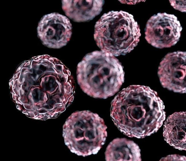
Biomimetic Nanoparticles for Targeted Cancer Therapy

Posted by in categories: biotech/medical, nanotechnology

Circa 2021


Novel fluorescence imaging assay provides new insights for developing more effective cancer nanomedicines.

Mar 22, 2022

All Charged Up: Engineers Create A Battery Made Of Wood

Posted by in category: nanotechnology

This doesn’t look like your trusty potato battery: a prototype device made by scientists at the University of Maryland uses wood fibers coated with carbon nanotubes to create an electric current.

Mar 21, 2022

So Where Exactly Are We With Nanotechnology? | Answers With Joe

Posted by in categories: nanotechnology, sustainability

Get a year of Nebula and Curiosity Stream for only $14.79 when you sign up at http://www.curiositystream.com/joescott.
We’ve been hearing for years how nanotechnology is going to change the world. In movies and in headlines, nanotechnology is almost like “future magic” that will make the impossible possible. But how realistic are those predictions? And how close are we to seeing some of them come true? Let’s take a look at the state of nanotechnology.

Want to support the channel? Here’s how:

Continue reading “So Where Exactly Are We With Nanotechnology? | Answers With Joe” »

Mar 20, 2022

Nanotechnology Repairs Engine Damage in Cars

Posted by in categories: materials, nanotechnology

NASA

That spot of oil on the garage floor dripping from your engine indicates a problem. It’s so small that you put off going to the mechanic, until you hear a new noise and the oil pressure warning light goes off. The bad news is that one of the bearings in the crankshaft is the source of the issue. Due to wear, the normally round part is now more elliptical in shape. Some of the metal has worn away, landing you with a costly repair.

This kind of wear on engine components is common because of friction, and it happens in all machinery with moving parts. Lubricants that reduce friction can only delay and minimize this inevitable damage. The idea of reversing that wear by fixing a worn part was the dream of Washington State University PhD candidate Pavlo “Pasha” Rudenko, who decided to research using smart nanoparticles to replace eroded material.

Mar 19, 2022

You’re invited to join our subreddit community —

Posted by in categories: bioengineering, biotech/medical, cyborgs, genetics, nanotechnology, robotics/AI, singularity, transhumanism, virtual reality

R/IntelligenceSupernova — dedicated to techno-optimists, singularitarians, transhumanist thinkers, cosmists, futurists, AI researchers, cyberneticists, crypto enthusiasts, VR creators, artists, philosophers of mind. Accelerating now towards the Cybernetic Singularity with unprecedented advances in AI & Cybernetics, VR, Biotechnology, Nanotechnology, Bionics, Genetic Engineering, Optogenetics, Neuroengineering, Robotics, and other IT fields.

Join now: https://www.reddit.com/r/IntelligenceSupernova.

#Subreddit #IntelligenceSupernova

Mar 17, 2022

Simpler graphene method paves way for new era of nanoelectronics

Posted by in categories: chemistry, nanotechnology, particle physics

Ever since its discovery in 2004, graphene has received attention owing to its extraordinary properties, among them its extremely high carrier mobility. However, the high carrier mobility has only been observed using techniques that require complex and expensive fabrication methods. Now, researchers at Chalmers report on a surprisingly high charge-carrier mobility of graphene using much cheaper and simpler methods.

“This finding shows that graphene transferred to cheap and flexible substrates can still have an uncompromisingly high mobility, and it paves the way for a new era of graphene nano-electronics,” says Munis Khan, researcher at Chalmers University of Technology.

Graphene is the one-atom-thick layer of carbon atoms, known as the world’s thinnest material. The material has become a popular choice in semiconductor, automotive and optoelectronic industry due to its excellent electrical, chemical, and material properties. One such property is its extremely .

Mar 17, 2022

Self-assembling and complex, nanoscale mesocrystals can be tuned for a variety of uses

Posted by in categories: biotech/medical, chemistry, nanotechnology, solar power

A research team from KTH Royal Institute of Technology and Max Planck Institute of Colloids and Interfaces reports to have found the key to controlled fabrication of cerium oxide mesocrystals. The research is a step forward in tuning nanomaterials that can serve a wide range of uses—including solar cells, fuel catalysts and even medicine.

Mesocrystals are nanoparticles with identical size, shape and crystallographic orientation, and they can be used as to create artificial nanostructures with customized optical, magnetic or electronic properties. In nature, these three-dimensional structures are found in coral, sea urchins and calcite desert rose, for example. Artificially-produced cerium oxide (CeO2) mesocrystals—or nanoceria—are well-known as catalysts, with antioxidant properties that could be useful in pharmaceutical development.

“To be able to fabricate CeO2 mesocrystals in a controlled way, one needs to understand the formation mechanism of these materials,” says Inna Soroka, a researcher in applied at KTH. She says the team used radiation chemistry to reveal for the first time the ceria mesocrystal formation mechanism.

Mar 17, 2022

Wax-coated sand keeps soil wet longer, improves crop yields in arid regions

Posted by in categories: biotech/medical, nanotechnology

Dry, hot regions are difficult places to grow plants because the soil dries out quickly. As a result, farmers in arid and semi-arid regions irrigate their fields with buried networks of irrigation tubing and cover the ground with plastic sheets. But plastic sheets are expensive and create waste. Now, researchers reporting in ACS Agricultural Science & Technology have developed a simple, biodegradable ground cover—wax-coated sand—which keeps soil wet and increases crop yields.

To irrigate crops, farmers usually get water from nearby waterways or underground aquifers. These supplies can be rapidly depleted when growing plants in , where the soil is comprised mostly of sand and can’t hold onto water well. One way to improve irrigated water’s efficiency is to make sure it stays in the soil long enough so that plants’ roots can take it up. Previous studies have shown that ground cover barriers, such as plastic sheets and engineered nanomaterials, can slow evaporation and enhance and . However, both could leach unwanted compounds into the soil with unknown long-term impacts. Some plants and animals naturally produce waxy substances that trap and pool water from fog or condensation so that they can access these moisture sources. Taking inspiration from nature, Himanshu Mishra and colleagues wanted to see if they could coat sand with wax, creating an environmentally benign ground cover to control soil evaporation.

The researchers chose purified paraffin wax, a biodegradable substance available in large quantities, for their experiments. They dissolved the wax in hexane and poured silica sand into the mixture. As the solvent evaporated, a 20-nm-thick coating of wax was left behind on the grains. When the team applied the wax-coated sand in a on an open field in Saudi Arabia, it decreased the loss of soil moisture up to 50–80%. Field trials revealed that tomato, barley and wheat plants mulched with the new material produced substantially more fruit and grain than those grown in uncovered soil. In addition, the microbial community around the plants’ roots and in the soil wasn’t negatively impacted by the waxy mulch, which could have acted as a food source for some of the microbes. This simple nature-inspired technology could make more efficient in arid regions, the researchers say.

Mar 14, 2022

Creating sub-1-nm gate lengths for MoS2 transistors

Posted by in categories: computing, nanotechnology, particle physics

A team of researchers working at Tsinghua University in China has created a sub-1-nm gate in a MoS2 transistor. In their paper published in the journal Nature, the group outlines how they created the super tiny gate and explains why they believe it will be difficult for anyone to beat their record.

For most of the history of microcomputing, Moore’s Law has held up—researchers and engineers have managed to double the speed and capability of computers regularly by reducing the size of their components. But more recently, it has grown increasingly difficult to make components smaller as scientists now run into . In this new effort, the researchers believe they may have bumped up against the ultimate limit—they have built a gate that is just one atom in length.

At their most basic, transistors are a source and a drain, with a gate controlling the flow of electricity between them. It switches on and off depending on how much electricity is applied. The push to reduce the size of the components has led to the testing of materials such as carbon nanotubes, which are approximately 1nm, for use as gates. In this new effort, the researchers have unrolled the and used its graphene edge as the gate—reducing its length to just 0.34 nm.

Mar 14, 2022

Scientists fabricate novel electrical component to improve stability of solar cells

Posted by in categories: internet, nanotechnology, solar power, sustainability

In the future, decarbonized societies that use internet of things (IoT) devices will become commonplace. But to achieve this, we need to first realize highly efficient and stable sources of renewable energy. Solar cells are considered a promising option, but their electrical contacts suffer from a “tradeoff” relationship between surface passivation and conductivity. Recently, researchers from Japan have developed a new type of electrical contact that can overcome this problem.

The most recent type of commercial photovoltaic cell (solar cell) uses stacked layers of crystalline silicon (c-Si) and an ultrathin layer of silicon oxide (SiOx) to form an electrical contact. The SiOx is used as a “passivating” film—an unreactive layer that improves the performance, reliability, and stability of the device. But that does not mean that simply increasing the thickness of this passivating layer will lead to improved . SiOx is an electrical insulator and there is a trade-off relationship between passivation and the conductivity of the electrical contact in solar cells.

In a new study, published in ACS Applied Nano Materials, a research team led by Assistant Professor Kazuhiro Gotoh and Professor Noritaka Usami from Nagoya University has developed a novel SiOx layer that simultaneously allows high passivation and improved conductivity. Named NAnocrystalling Transport path in Ultrathin dielectrics for REinforcing passivating contact (NATURE contact), the new electrical contact consists of three-layer structures made up of a layer of silicon nanoparticles sandwiched between two layers of oxygen-rich SiOx. “You can think of a passivating film as a big wall with gates in it. In the NATURE contact, the big wall is the SiOx layer and the gates are Si nanocrystals,” explains Dr. Gotoh.