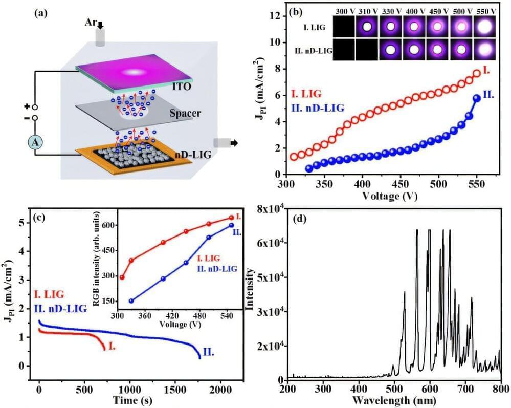
Menu

Blog

Archive for the ‘nanotechnology’ category: Page 100

May 11, 2022

A simpler approach for creating quantum materials

Posted by in categories: nanotechnology, quantum physics

Since graphene was first isolated and characterized in the early 2000s, researchers have been exploring ways to use this atomically thin nanomaterial because of its unique properties such as high tensile strength and conductivity.

In more recent years, twisted bilayer graphene, made of two sheets of graphene twisted to a specific “magic” angle, has been shown to have superconductivity, meaning that it can conduct electricity with very little resistance. However, using this approach to make devices remains challenging because of the low yield of fabricating twisted bilayer graphene.

Now, a new study shows how patterned, periodic deformations of a single layer of graphene transforms it into a material with previously seen in twisted graphene bilayers. This system also hosts additional unexpected and interesting conducting states at the boundary. Through a better understanding of how unique properties occur when single sheets of graphene are subjected to periodic strain, this work has the potential to create quantum devices such as orbital magnets and superconductors in the future. The study, published in Physical Review Letters, was conducted by graduate student Võ Tiến Phong and professor Eugene Mele in Penn’s Department of Physics & Astronomy in the School of Arts & Sciences.

May 11, 2022

Nature-inspired self-sensing materials could lead to new developments in engineering

Posted by in categories: engineering, health, nanotechnology

The cellular forms of natural materials are the inspiration behind a new lightweight, 3D printed smart architected material developed by an international team of engineers.

The team, led by engineers from the University of Glasgow, mixed a common form of industrial plastic with carbon nanotubes to create a material which is tougher, stronger and smarter than comparable conventional materials.

The nanotubes also allow the otherwise nonconductive plastic to carry an throughout its structure. When the structure is subjected to mechanical loads, its electrical resistance changes. This phenomenon, known as piezoresitivity, gives the material the ability to “sense” its structural health.

May 11, 2022

Design of effective self-powered SnS2/halide perovskite photo-detection system based on triboelectric nanogenerator

Posted by in categories: chemistry, health, internet, nanotechnology, robotics/AI, wearables

On account of the improvement the Internet of things (IoTs) and smart devices, our lives have been noticeably facilitated in the past few years. Machines and devices are becoming more ingenious with the help of artificial intelligence and various sensors1,2. So, integrated circuits are necessary to provide convenient and effectual communication3 Since the first report on TENG by Wang’s group in 20124, triboelectric systems have been recognized as a proper choice to harvest and convert the energy from the environment5,6. Photodetectors, as one of the most significant types of sensors that can precisely convert incident light into electrical signals have attracted increasing attention in recent years. Various applications including photo-sensors, spectral analysis7,8, environment monitoring9, communication devices10, imaging11, take advantage of narrow band or broad band photodetectors from ultraviolet to terahertz wavelenght. Literature reviews show that the heterojunction/heterostructure based on 2D/3D materials have been widely used in PD applications. In fact, to attain high performance of PDs based heterojunction, the built-in electrical field is needed to suppress the photogenerated recombination and stimulating collection12. Although, Si based PDs offer reliably high performance results, their complexity and expensive manufacturing process have limited their expansion and adoptability for industrial purposes13,14,15. Hence, most available PDs are designed based on external power supplies such as electrochemical batteries for signal production and processing, their design not only increases the sensor’s dimension and weight, but also creates limitations for sensor maintenances16 which is not proper in the IoTs. In 2014, ZH Lin et al. and Zheng et al. represented an investigation on the self-powered PD based on TENG system3,17, and since then, self-driven PDs have been extensively investigated2,5,9,18,19,20. These devices can find potential applications in health monitoring systems such as heart checking21 and health protection from some detrimental radiation such as high levels of UV radiance22.

But in the other hand, even though TENGs could be promise for using in wearable electronics, they still inevitably have limitations in power generation, sensing range, sensitivity, and also the sensing domain for the intrinsic limitations of electrification23,24,25. Moreover, due to high voltage, low current, and alternating current output of the TENGs, they cannot be used in order to supply power to electronic devices effectively without using power management circuits (PMCs) based on the LC modules. There are several reports that describe the importance of the impedance matching of the TENG and PMC units for better energy storage efficiency of the pulsed-TENG26,27. Without using the PMC unit, there are some challenges as a result of synching the TENG, as the power supply, and the consumption element such as the PD device. These challenges include the process of matching the resistance of the device and the impedance of the TENG to achieve effective performance of the self-powered system6,28.

In this study an efficient battery-free photodetector based on bulk heterojunction SnS2 nanosheets and perovskite materials has been designed and powered employing three different TENGs (GO paper/ Kapton, FTO/Kapton and hand/ FTO). In the first step for circuit designing to have better performance of the photodetector in coupling with TENG, the effect load resistance amount in the circuit on the impedance matching the TENG and the inner resistance of the photodetector, has been investigated through output current amplitude. The investigation, shows that to achieve the high amount of the photocurrent, the load resistance should be positioned in both critical zone of the out-put voltage of the TENG and the resistance range of high power density production of the TENG. In the second step, for investigation the effect of the dark resistance of the photodetector on out-put current of the self-powered photodetector, a device with very lower initial resistance (All-oxide Cu2O/ZnO photodetector) has been used with and without different load resistance in the circuit; in this regard, it is concluding that the initial resistance is too important to have proper design impedance matching circuit.

May 11, 2022

Promising New Carbon Nanotube Chip for Cancer Cell Capture and Release

Posted by in categories: biotech/medical, computing, nanotechnology

A new two component-based glass/polydimethylsiloxane microfluidic pH-responsive carbon nanotube chip can efficiently capture or release cancer cells from blood samples.

May 10, 2022

Scientists develop powerful family of 2D materials

Posted by in categories: materials, nanotechnology

A team from the Tulane University School of Science and Engineering has developed a new family of two-dimensional materials that researchers say has promising applications, including in advanced electronics and high-capacity batteries.

Led by Michael Naguib, an assistant professor in the Department of Physics and Engineering Physics, the study has been published in the journal Advanced Materials.

“Two-dimensional are nanomaterials with thickness in the nanometer size (nanometer is one millionth of a millimeter) and lateral dimensions thousands of times the thickness,” Naguib said. “Their flatness offers unique set of properties compared to bulk materials.”

May 9, 2022

Cryostasis Revival: The Recovery of Cryonics Patients through Nanomedicine

Posted by in categories: biotech/medical, computing, cryonics, life extension, nanotechnology

Cryostasis Revival by Robert Freitas is the first comprehensive technical exposition how to revive cryonics patients in the future. This 700+ page book with thousands of references, and technical color illustrations, is now available on Amazon in a limited textbook hardcover edition.


Cryostasis is an emergency medical procedure in which a human patient is placed in biological stasis at cryogenic temperatures. A cryopreserved patient can be maintained in this condition indefinitely without suffering additional degradation, but cannot yet be revived using currently available technology. This book presents the first comprehensive conceptual protocol for revival from human cryopreservation, using medical nanorobots. The revival methods presented in this book involve three stages: collecting information from preserved structure, computing how to fix damaged structure, and implementing the repair procedure using nanorobots manufactured in a nanofactory – a system for atomically precise manufacturing that is now visible on the technological horizon.

May 8, 2022

‘Nanomagnetic’ computing can provide low-energy AI, researchers show

Posted by in categories: biotech/medical, nanotechnology, robotics/AI

Researchers have shown it is possible to perform artificial intelligence using tiny nanomagnets that interact like neurons in the brain.

The new method, developed by a team led by Imperial College London researchers, could slash the of (AI), which is currently doubling globally every 3.5 months.

In a paper published today in Nature Nanotechnology, the international team have produced the first proof that networks of nanomagnets can be used to perform AI-like processing. The researchers showed nanomagnets can be used for ‘time-series prediction’ tasks, such as predicting and regulating insulin levels in .

Apr 28, 2022

World’s smallest gears measure mere nanometers to power molecular machines

Posted by in categories: biotech/medical, nanotechnology

In many fields of technology, smaller is better, and machinery is now getting so tiny it’s measured in mere atoms. Researchers at the University of Erlangen–Nuremberg (FAU) in Germany have now developed what they claim are the world’s smallest working gear wheels.

Molecular machines and nanorobots could be extremely useful in the coming decades, helping to construct electronic components, transport drugs through the body, or manipulate individual cells or molecules.

To that end, scientists have developed nanoscale versions of many machine parts, such as motors, pistons, pumps, wrenches and propellers.

Apr 27, 2022

A DNA molecular printer capable of programmable positioning and patterning in two dimensions

Posted by in categories: biotech/medical, nanotechnology

A nanoscale machine made from DNA moves under external control and prints by selectively modifying pixels on a canvas.

Apr 27, 2022

Honeycomb-like nanopatterning boosts efficiency of ultrathin solar panels

Posted by in categories: nanotechnology, solar power, sustainability

“Hyperuniform disordered” design delivers 66.5% solar absorption.

Page 100 of 272First979899100101102103104Last