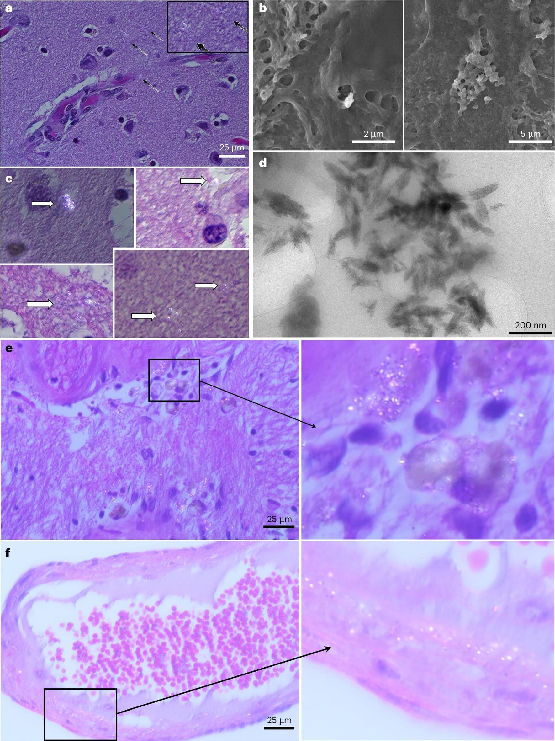
Tiny plastic particles may accumulate at higher levels in the human brain than in the kidney and liver, with greater concentrations detected in postmortem samples from 2024 than in those from 2016, suggests a paper published in Nature Medicine. Although the potential implications for human health remain unclear, these findings may highlight a consequence of rising global concentrations of environmental plastics.
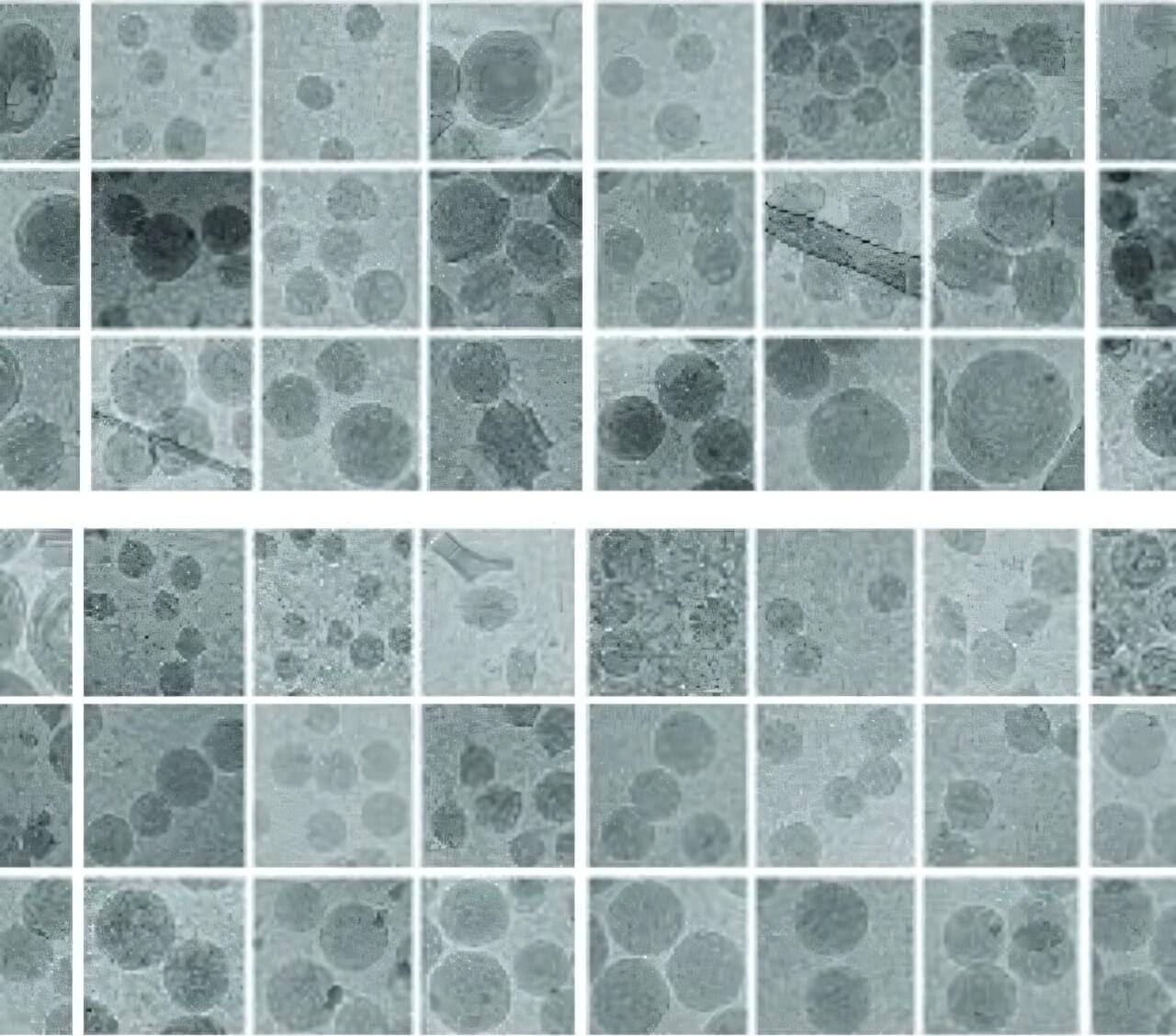
The amount of environmental plastic nano-and microparticles, which range in size from as small as 1 nanometer (one billionth of a meter) up to 500 micrometers (one millionth of a meter) in diameter, has increased exponentially over the past 50 years. However, whether they are harmful or toxic to humans is unclear. Most previous studies used visual microscopic spectroscopy methods to identify particulates in human tissues, but this is often limited to particulates larger than 5 micrometers.
Researcher Matthew Campen and colleagues used novel methods to analyze the distribution of micro-and nanoparticles in samples of liver, kidney, and brain tissues from human bodies that underwent autopsy in 2016 and 2024. A total of 52 brain specimens (28 in 2016 and 24 in 2024) were analyzed.