Category: nanotechnology – Page 94

Nanotechnology: A potential cure for incurable diseases
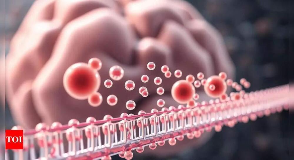
Nanotechnology is poised to transform neurological disorder treatments by overcoming the blood-brain barrier, enabling effective medication delivery for conditions like dementia and Alzheimer’s. This innovative approach also shows promise in dermatology and cancer treatment, enhancing drug absorption and targeting, while minimizing side effects. Experts at AIIMS highlighted ongoing research and potential breakthroughs expected in the next few years.

An Expert Explains The Real Dangers of Microplastics to Human Health
It’s no secret: when we savour a delicious piece of fish or a platter of seafood, we’re not just consuming valuable omega-3s and vitamin D. Alongside these benefits come less appetising elements – countless micro– and nano-plastics.
These plastic particles, measuring less than 5 millimetres, enter our oceans through human waste and penetrate the food chain. According to an Ifremer study, around 24,400 billion microplastics are floating on the ocean’s surface.
These particles are found in all marine organisms – from microalgae to fish, which occupy higher levels of the food chain. This phenomenon not only threatens marine ecosystems but also raises concerns about potential risks to human health.
Nano-scale dinosaur made by Australian researchers from DNA building blocks
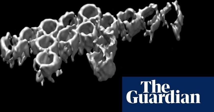
Australian researchers have created building blocks out of DNA to construct a series of nano-scale objects and shapes, from a rod and a square to an infinitesimally small dinosaur.
The approach turns DNA into a modular material for building nanostructures – thousands of times narrower than a human hair. Developed by researchers from the University of Sydney Nano Institute and published in the journal Science Robotics, it suggests exciting possibilities for future use of nanobot technology.
Smart Materials and Nanotechnology Engineering conf. kicks off
Dr Mehdi Ghommem said that the AUS was happy to host and organise the eighth edition of the International Conference on Smart Materials and Nanotechnology, and to host more than 100 participants from 15 different countries.
Ghommem added that the social programme of the conference included plenary lectures, keynote lectures, parallel technical sessions with more than 70 presentations.
Dr Mehdi Ghommem also explained that the social programme which came in parallel with the technical programme included dinner, a visit of iconic landmark in Sharjah. He stressed that it was a great opportunity for participants not only to interact and talk about scientific topics, but also to get to know about the local culture and also, to get good exposure to the main monuments of Sharjah.
Nanorobot hand made of DNA grabs viruses for diagnostics and blocks cell entry
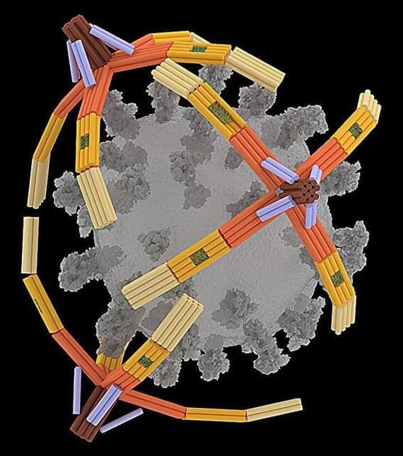
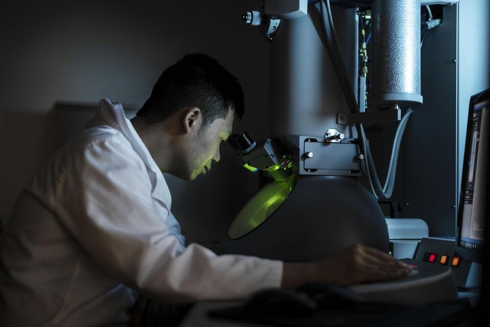
A tiny, four-fingered “hand” folded from a single piece of DNA can pick up the virus that causes COVID-19 for highly sensitive rapid detection and can even block viral particles from entering cells to infect them, University of Illinois Urbana-Champaign researchers report. Dubbed the NanoGripper, the nanorobotic hand also could be programmed to interact with other viruses or to recognize cell surface markers for targeted drug delivery, such as for cancer treatment.
Led by Xing Wang, a professor of bioengineering and of chemistry at the U. of I., the researchers describe their advance in the journal Science Robotics.
Inspired by the gripping power of the human hand and bird claws, the researchers designed the NanoGripper with four bendable fingers and a palm, all in one nanostructure folded from a single piece of DNA. Each finger has three joints, like a human finger, and the angle and degree of bending are determined by the design on the DNA scaffold.
Nanostructures pave the way for advanced robotics—and mini dinosaurs
Researchers at the University of Sydney Nano Institute have made a significant advance in the field of molecular robotics by developing custom-designed and programmable nanostructures using DNA origami.
This innovative approach has potential across a range of applications, from targeted drug delivery systems to responsive materials and energy-efficient optical signal processing. The method uses “DNA origami,” so-called as it uses the natural folding power of DNA, the building blocks of human life, to create new and useful biological structures.
As a proof-of-concept, the researchers made more than 50 nanoscale objects, including a “nano-dinosaur,” a “dancing robot” and a mini-Australia that is 150 nanometers wide, a thousand times narrower than a human hair.

Bio Tech Dominates Research Schedule to Advance Space, Earth Industries
The Expedition 72 crew studied micro-algae and DNA-like nanomaterials on Tuesday to improve health in space and on Earth. The orbital residents also worked on cargo transfers and lab maintenance aboard the International Space Station.
NASA Flight Engineer Nick Hague began his day processing radiation-resistant samples of Arthrospira C micro-algae and stowing them in an incubator for analysis. The samples will be exposed to different light intensities to observe how they affect the micro-algae’s cell growth and oxygen production. Results may advance the development of spacecraft life support systems and fresh food production in space.
Afterward, Hague joined Commander Suni Williams of NASA for a different research session mixing water with samples of messenger RNA, or mRNA, and protein to create DNA-like nanomaterial products inside the Kibo laboratory module’s Life Science Glovebox. Flight Engineer Butch Wilmore then transferred the samples, exposed them to ultrasonic waves, and imaged them with a spectrophotometer to measure the intensity of light at different wavelengths and evaluate the quality of the nanomaterials. The samples will also be returned to Earth for further evaluation. Results may lead to improved therapies for Earth and space health conditions as well as advance the space economy.
Study finds ZnO nanorods achieve 98.3% Faraday efficiency in CO₂ reduction
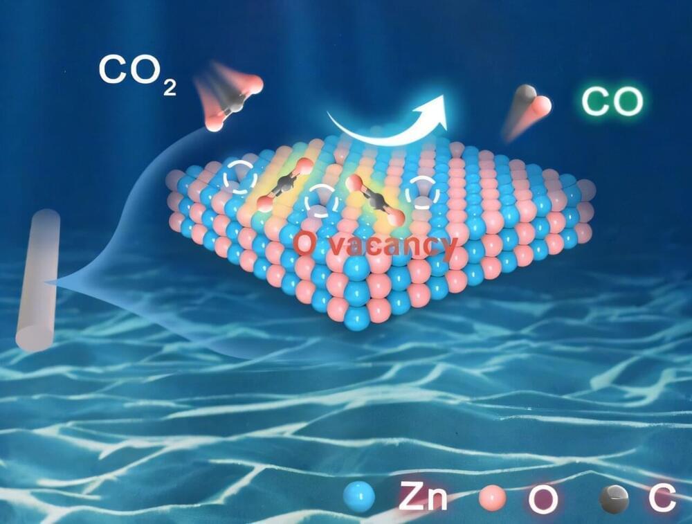
Nano-ZnO is a potential catalyst material for carbon dioxide electrocatalytic reduction (CO2RR), but its effective Faraday efficiency (FE) is still below 90% and the current density is less than 300 mA cm-2, which is not enough to meet industrial requirements.
A new study published in Chem Catalysis reported on ZnO nanorods for electrocatalytic CO2RR, which after 500°C heat-treatment, achieved the highest oxygen vacancy content, the highest FECO of 98.3%, and a partial current density of 786.56 mA cm-2 in a 3 M KCl electrolyte.
The research was conducted by Prof. Wu Zhonghua and Dr. Xing Xueqing from the Institute of High Energy Physics of the Chinese Academy of Sciences (CAS) and Prof. Han Buxing from the Institute of Chemistry of CAS.
Synthetic Genes Engineered to Mimic how Cells Build Tissues and Structures
Advance paves the way for broad applications in medicine and biotech. Researchers from the UCLA Samueli School of Engineering and the University of Rome Tor Vergata in Italy have developed synthetic genes that function like the genes in living cells.
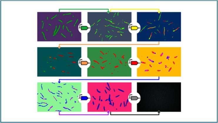
The artificial genes can build intracellular structures through a cascading sequence that builds self-assembling structures piece by piece. The approach is similar to building furniture with modular units, much like those found at IKEA. Using the same parts, one can build many different things and it’s easy to take the set apart and reconstruct the parts for something else. The discovery offers a path toward using a suite of simple building blocks that can be programmed to make complex biomolecular materials, such as nanoscale tubes from DNA tiles. The same components can also be programmed to break up the design for different materials.
The research study was recently published in Nature Communications and led by Elisa Franco, a professor of mechanical and aerospace engineering and bioengineering at UCLA Samueli. Daniela Sorrentino, a postdoctoral scholar in Franco’s Dynamic Nucleic Acid Systems lab, is the study’s first author.