Toggle light / dark theme

Researchers develop gold nanowire spectroscopy system to reveal how trions are generated

In a significant advancement for next-generation semiconductors, a collaborative research team has made groundbreaking discoveries in the field of two-dimensional (2D) semiconductors.

Their findings, published in Nano Letters, shed light on the generation and control of trions, providing valuable insights into the optical properties of these materials.

2D semiconductors, known for their exceptional light characteristics per unit volume with high flexibility due to their atomic layer thickness, hold immense potential for applications in areas such as advanced flexible devices, nano photonics, and solar cells.

Sub-Wavelength Light Confinement Demonstrated in New III-V Semiconductor Nanocavity

New nanocavities pave the way for enhanced nanoscale lasers and LEDs that could enable faster data transmission using smaller, more energy-efficient devices.

As we transition to a new era in computing, there is a need for new devices that integrate electronic and photonic functionalities at the nanoscale while enhancing the interaction between photons and electrons. In an important step toward fulfilling this need, researchers have developed a new III-V semiconductor nanocavity that confines light at levels below the so-called diffraction limit.

“Nanocavities with ultrasmall mode volumes hold great promise for improving a wide range of photonic devices and technologies, from lasers and LEDs to quantum communication and sensing, while also opening up possibilities in emerging fields such as quantum computing,” said the leading author Meng Xiong from the Technical University of Denmark. “For example, light sources based on these nanocavities could significantly improve communication by enabling faster data transmission and strongly reduced energy consumption.

New Medicine can Create a New Life for Diabetes Patients—Without Needles

There are approximately 425 million people worldwide with diabetes. Approximately 75 million of these inject themselves with insulin daily. Now, they may soon have a new alternative to syringes or insulin pumps. Scientists have found a new way to supply the body with smart insulin.

The new insulin can be eaten by taking a capsule or, even better, within a piece of chocolate.

Inside these are tiny nano-carriers in which the insulin is encapsulated. The particles are 1/10,000th the width of a human hair and so small that you cannot even see them under a normal microscope.

A nanotechnology‐based CRISPR/Cas9 delivery system for genome editing in cancer treatment

In the presence of protospacer adjacent motif (PAM), sgRNA accurately leads the Cas9 endonuclease to the target regions, where it causes DNA double strand breaks (DSBs), resulting in site‐specific genomic change. Endogenous DNA repair can take place following the creation of a DSB via two primary genome editing pathways: nonhomologous end joining (NHEJ) or homology‐directed repair (HDR).

By using the biological characteristics of Cas9 targeting specific DNA sequences under the guidance of sgRNA, scientists have further developed gene targeting activation and gene targeting inhibition tools based on dCas9, called CRISPRa and CRISPRi respectively.

In the paper, characteristics of three forms of CRISPR/Cas9 cargos are outlined. Three delivery forms of the CRISPR/Cas9 system are plasmids, mRNA/sgRNA, and ribonucleoprotein (RNP) complexes, each of which has its own advantages and disadvantages.

Study unveils key dynamics of 2D nanomaterials with view to larger-scale production

A team of Rice University researchers mapped out how flecks of 2D materials move in liquid ⎯ knowledge that could help scientists assemble macroscopic-scale materials with the same useful properties as their 2D counterparts.

“Two-dimensional nanomaterials are extremely thin—only several atoms thick—sheet-shaped materials,” said Utana Umezaki, a Rice graduate student who is a lead author on a study published in ACS Nano. “They behave very differently from materials we’re used to in daily life and can have really useful properties: They can withstand a lot of force, resist high temperatures and so on. To take advantage of these unique properties, we have to find ways to turn them into larger-scale materials like films and fibers.”

In order to maintain their special properties in bulk form, sheets of 2D materials have to be properly aligned ⎯ a process that often occurs in solution phase. Rice researchers focused on graphene, which is made up of , and hexagonal boron nitride, a material with a similar structure to graphene but composed of boron and nitrogen atoms.

Automated Atomic Force Microscope To Make 3D Nanoscale Data More Accessible

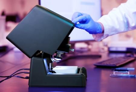
ICSPI, a leader in benchtop nanoscale imaging instruments, has announced the launch of its new Redux AFM, an automated atomic force microscope (AFM) designed to allow scientists and engineers to effortlessly collect 3-dimensional data at the nanoscale.

ICSPI’s mission is to expand access to nanoscale measurement with powerful, automated and intuitive imaging tools. Building on the success of its nGauge AFM, of which hundreds of units are in operation in over 30 countries, ICSPI is excited to introduce the Redux AFM and elevate the user experience of nanoscale imaging with automation.

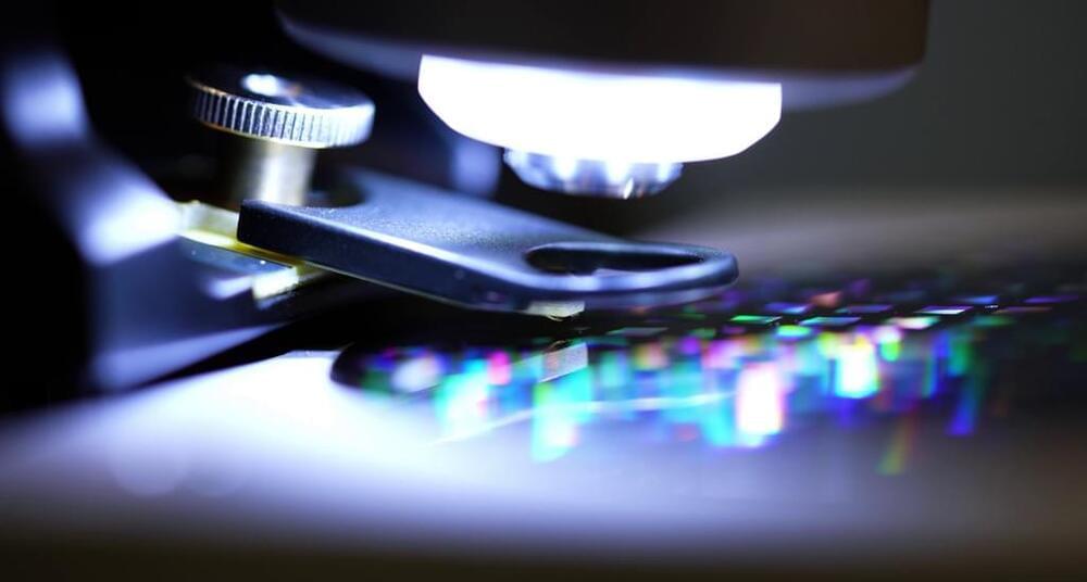
Traditional AFM instruments, while powerful for nanoscale surface imaging, are often hindered by complex and time-consuming setup processes which are rooted in technology developed in the 1980s. Recognizing this challenge, ICSPI revolutionized the landscape with its unique AFM-on-a-chip technology. The Redux AFM, harnessing this breakthrough technology, makes nanoscale imaging effortless. By integrating multiple components onto a single chip, the Redux eliminates the cumbersome aspects of traditional AFM, such as silicon probe exchange, cantilever alignment, tip crashes, tip-sample approach, and controller tuning.

Researchers showcase new breakthroughs for unlocking the potential of plasmonics

Plasmonics are special optical phenomena that are understood as interactions between light and matter and possess diverse shapes, material compositions, and symmetry-related behavior. The design of such plasmonic structures at the nanoscale level can pave the way for optical materials that respond to the orientation of light (polarization), which is not easily achievable in bulk size and existing materials.

In this regard, “shadow growth” is a technique that utilizes vacuum deposition to produce nanoparticles from a wide range of 2D and 3D shapes at nanoscale. Recent research progress in controlling this shadow effect has broadened the possibilities for the creation of different nanostructures.

Now, in twin studies led by Assistant Professor Hyeon-Ho Jeong from the Gwangju Institute of Science and Technology (GIST), Republic of Korea, researchers have comprehensively shed light on the recent advances in shadow growth techniques for hybrid plasmonic nanomaterials, including clock-inspired designs containing magnesium (Mg).