In recent years, technological advancements have made it possible to create synthetic diamonds that have similar physical and chemical properties to natural diamonds. While synthetic diamonds are not considered “fake” or “imitation,” they are often more affordable than their natural counterparts, making them a popular choice for those who want the beauty of a diamond without the high cost. Synthetic diamonds are also often more environmentally friendly, as they do not require the same level of mining and extraction as natural diamonds.
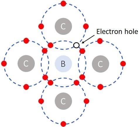
In its pristine state, diamond is a non-conductive material, devoid of free electrons or “holes” that can facilitate electrical conduction (Figure 1). However, by introducing boron atoms into the diamond crystal lattice, its optical and electrical properties can be significantly altered. As the concentration of boron is increased, the diamond’s color shifts from its characteristic clear hue to a delicate shade of blue, while its electrical conductivity transforms from an insulator to a semiconductor.
Further increases in the boron content result in a lustrous blue shade that resembles the sheen of metallic surfaces and eventually culminates in a deep, ebony coloration. Such heavily boron-doped diamond (BDD) is also as electrically conducting as some metals, and at low temperatures, exhibits superconductivity, allowing electrical conduction with no resistance.
