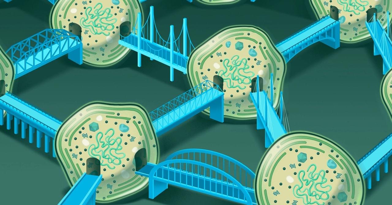
Toggle light / dark theme

Regenerative nanochip restores ANY tissue with 98% success and clinical trials start next year

Year 2017 face_with_colon_three


Tissue Nanotransfection (TNT), that can generate any cell type of interest for treatment within the patient’s own body. This technology may be used to repair injured tissue or restore function of aging tissue, including organs, blood vessels and nerve cells.

“By using our novel nanochip technology, injured or compromised organs can be replaced. We have shown that skin is a fertile land where we can grow the elements of any organ that is declining,” said Dr. Chandan Sen, director of Ohio State’s Center for Regenerative Medicine & Cell Based Therapies, who co-led the study with L. James Lee, professor of chemical and biomolecular engineering with Ohio State’s College of Engineering in collaboration with Ohio State’s Nanoscale Science and Engineering Center.

Researchers studied mice and pigs in these experiments. In the study, researchers were able to reprogram skin cells to become vascular cells in badly injured legs that lacked blood flow. Within one week, active blood vessels appeared in the injured leg, and by the second week, the leg was saved. In lab tests, this technology was also shown to reprogram skin cells in the live body into nerve cells that were injected into brain-injured mice to help them recover from stroke.

Recovering lossless propagation: HKU physicists overcoming optical loss in polariton system with synthetic complex frequency waves

A collaborative research team co-led by Professor Shuang ZHANG, the Interim Head of the Department of Physics, The University of Hong Kong (HKU), along with Professor Qing DAI from National Center for Nanoscience and Technology, China, has introduced a solution to a prevalent issue in the realm of nanophotonics – the study of light at an extremely small scale. Their findings, recently published in the prestigious academic journal Nature Materials, propose a synthetic complex frequency wave (CFW) approach to address optical loss in polariton propagation. These findings offer practical solutions such as more efficient light-based devices for faster and more compact data storage and processing in devices such as computer chips and data storage devices, and improved accuracy in sensors, imaging techniques, and security systems.

Surface plasmon polaritons and phonon polaritons offer advantages such as efficient energy storage, local field enhancement, and high sensitivities, benefitting from their ability to confine light at small scales. However, their practical applications are hindered by the issue of ohmic loss, which causes energy dissipation when interacting with natural materials.

Over the past three decades, this limitation has impeded progress in nanophotonics for sensing, superimaging, and nanophotonic circuits. Overcoming ohmic loss would significantly enhance device performance, enabling advancement in sensing technology, high-resolution imaging, and advanced nanophotonic circuits.

A ghostly quasiparticle rooted in a century-old Italian mystery could unlock quantum computing’s potential—if only it could be pinned down

Already, the graphene efforts have offered “a breath of fresh air” to the community, Alicea says. “It’s one of the most promising avenues that I’ve seen in a while.” Since leaving Microsoft, Zaletel has shifted his focus to graphene. “It’s clear that this is just where you should do it now,” he says.

But not everyone believes they will have enough control over the free-moving quasiparticles in the graphene system to scale up to an array of qubits—or that they can create big enough gaps to keep out intruders. Manipulating the quarter-charge quasiparticles in graphene is much more complicated than moving the Majoranas at the ends of nanowires, Kouwenhoven says. “It’s super interesting for physics, but for a quantum computer I don’t see it.”

Just across the parking lot from Station Q’s new office, a third kind of Majorana hunt is underway. In an unassuming black building branded Google AI Quantum, past the company rock-climbing wall and surfboard rack, a dozen or so proto–quantum computers dangle from workstations, hidden inside their chandelier-like cooling systems. Their chips contain arrays of dozens of qubits based on a more conventional technology: tiny loops of superconducting wires through which current oscillates between two electrical states. These qubits, like other standard approaches, are beset with errors, but Google researchers are hoping they can marry the Majorana’s innate error protection to their quantum chip.

Nanoscale Power Plants: Turning Heat Into Power With Graphene Ribbons

Quantum physicist Mickael Perrin uses graphene ribbons to build nanoscale power plants that turn waste heat from electrical equipment into electricity.

When Mickael Perrin started out on his scientific career 12 years ago, he had no way of knowing he was conducting research in an area that would be attracting wide public interest only a few years later: quantum electronics.

“At the time, physicists were just starting to talk about the potential of quantum technologies and quantum computers,” he recalls. “Today there are dozens of start-ups in this area, and governments and companies are investing billions in developing the technology further. We are now seeing the first applications in computer science, cryptography, communications, and sensors.”

Turning glass into a ‘transparent’ light-energy harvester

What happens when you expose tellurite glass to femtosecond laser light? That’s the question that Gözden Torun at the Galatea Lab at Ecole Polytechnique Federale de Lausanne, in collaboration with Tokyo Tech scientists, aimed to answer in her thesis work when she made the discovery that may one day turn windows into single material light-harvesting and sensing devices. The results are published in Physical Review Applied.

Interested in how the atoms in the tellurite would reorganize when exposed to fast pulses of high energy femtosecond laser light, the scientists stumbled upon the formation of nanoscale tellurium and tellurium oxide crystals, both etched into the glass, precisely where the glass had been exposed. That was the eureka moment for the scientists, since a semiconducting material exposed to daylight may lead to the generation of electricity.

“Tellurium being semiconducting, based on this finding we wondered if it would be possible to write durable patterns on the tellurite glass surface that could reliably induce electricity when exposed to light, and the answer is yes,” explains Yves Bellouard who runs EPFL’s Galatea Laboratory. “An interesting twist to the technique is that no additional materials are needed in the process. All you need is tellurite glass and a femtosecond laser to make an active photoconductive material.”

Advanced full-color image sensor technology enables simultaneous energy harvesting and imaging

Organic-based optoelectronic technology is increasingly recognized as an energy-efficient solution for low-power indoor electronics and wireless IoT sensors. This is largely due to its superior flexibility and light weight compared to conventional silicon-based devices. Notably, organic photovoltaic cells (OPVs) and organic photodetectors (OPDs) are leading examples in this field.

OPVs have the remarkable ability to absorb energy and generate electricity even under very low light conditions, while OPDs are capable of capturing images. However, despite their potential, the development of these devices has thus far been conducted independently. As a result, they have not yet reached the level of efficiency necessary to be considered practical for next-generation, miniaturized devices.

A Korea Institute of Science and Technology (KIST) research team, led by Dr. Min-Chul Park and Dr. Do Kyung Hwang of the Center for Opto-Electronic Materials and Devices, Prof. Jae Won Shim and Prof. Tae Geun Kim of the School of Electrical Engineering at Korea University, Prof. JaeHong Park of the Department of Chemistry and Nanoscience at Ewha Womans University, have now developed an organic-based optoelectronic device.