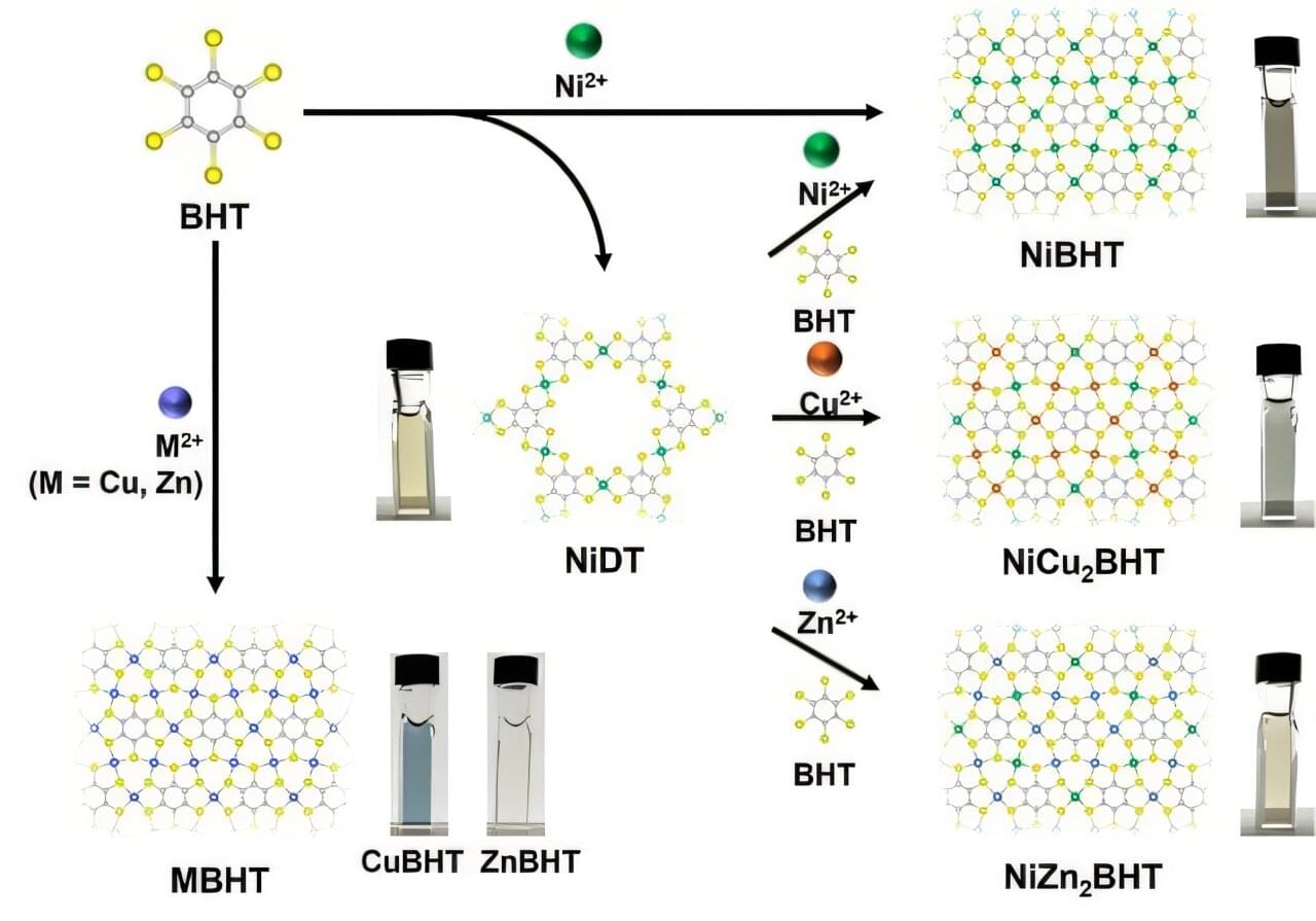
Menu

Blog

Archive for the ‘nanotechnology’ category: Page 62

Jun 24, 2023

Wearable energy harvesting-storage hybrid textiles as on-body self-charging power systems

Posted by in categories: energy, nanotechnology, sustainability, wearables

The rapid development of wearable electronics requires its energy supply part to be flexible, wearable, integratable and sustainable. However, some of the energy supply units cannot meet these requirements at the same time, and there is also a capacity limitation of the energy storage units, and the development of sustainable wearable self-charging power supplies is crucial. Here, we report a wearable sustainable energy harvesting-storage hybrid self-charging power textile. The power textile consists of a coaxial fiber-shaped polylactic acid/reduced graphene oxide/polypyrrole (PLA-rGO-PPy) triboelectric nanogenerator (fiber-TENG) that can harvest low-frequency and irregular energy during human motion as a power generation unit, and a novel coaxial fiber-shaped supercapacitor (fiber-SC) prepared by functionalized loading of a wet-spinning graphene oxide fiber as an energy storage unit. The fiber-TENG is flexible, knittable, wearable and adaptable for integration with various portable electronics. The coaxial fiber-SC has high volumetric energy density and good cycling stability. The fiber-TENG and fiber-SC are flexible yarn structures for wearable continuous human movement energy harvesting and storage as on-body self-charging power systems, with light-weight, ease of preparation, great portability and wide applicability. The integrated power textile can provide an efficient route for sustainable working of wearable electronics.

Jun 23, 2023

Flow of water on a carbon surface is governed by quantum friction, says study

Posted by in categories: computing, nanotechnology, particle physics, quantum physics, sustainability

Water and carbon make a quantum couple: the flow of water on a carbon surface is governed by an unusual phenomenon dubbed quantum friction. A new work published in Nature Nanotechnology experimentally demonstrates this phenomenon—which was predicted in a previous theoretical study—at the interface between liquid water and graphene, a single layer of carbon atoms. Advanced ultrafast techniques were used to perform this study. These results could lead to applications in water purification and desalination processes and maybe even to liquid-based computers.

For the last 20 years, scientists have been puzzled by how water behaves near carbon surfaces. It may flow much faster than expected from conventional flow theories or form strange arrangements such as square ice. Now, an international team of researchers from the Max Plank Institute for Polymer Research of Mainz (Germany), the Catalan Institute of Nanoscience and Nanotechnology (ICN2, Spain), and the University of Manchester (England), reports in the study published in Nature Nanotechnology on June 22, 2023, that water can interact directly with the carbon’s electrons—a quantum phenomenon that is very unusual in .

A liquid, such as water, is made up of that randomly move and constantly collide with each other. A solid, in contrast, is made of neatly arranged atoms that bathe in a cloud of electrons. The solid and the liquid worlds are assumed to interact only through collisions of the liquid molecules with the solid’s atoms—the liquid molecules do not “see” the solid’s electrons. Nevertheless, just over a year ago, a paradigm-shifting theoretical study proposed that at the water-carbon interface, the liquid’s molecules and the solid’s electrons push and pull on each other, slowing down the liquid flow: this new effect was called quantum friction. However, the theoretical proposal lacked experimental verification.

Jun 23, 2023

Researchers solve temperature problem for source-gated transistors

Posted by in categories: computing, engineering, nanotechnology

Low-cost, flexible displays that use very little energy could be a step closer, thanks to an innovation from the University of Surrey that solves a problem that has plagued source-gated transistors (SGT). The study has been published by IEEE Transactions on Electron Devices.

Dr. Radu Sporea, project lead from the University of Surrey, said, We used a rapidly emerging semiconductor material called IGZO or indium-gallium-zinc oxide to create the next generation of source-gated transistors. Through nanoscale contact engineering, we obtained transistors that are much more stable with temperature than previous attempts. Device simulations allowed us to understand this effect.

This new design adds to SGTs and retains usual benefits like using low power, producing high signal amplification, and being more reliable under different conditions. While source-gated transistors are not mainstream because of a handful of performance limitations, we are steadily chipping away at their shortcomings.

Jun 21, 2023

Extreme DNA resolution: Spatially multiplexed single-molecule translocations through a nanopore at controlled speeds

Posted by in categories: biotech/medical, genetics, nanotechnology

Aleksandra Radenovic, head of the Laboratory of Nanoscale Biology in the School of Engineering, has worked for years to improve nanopore technology, which involves passing a molecule like DNA through a tiny pore in a membrane to measure an ionic current. Scientists can determine DNA’s sequence of nucleotides—which encodes genetic information—by analyzing how each one perturbs this current as it passes through. The research has been published in Nature Nanotechnology.

Currently, the passage of molecules through a and the timing of their analysis are influenced by random physical forces, and the rapid movement of molecules makes achieving high analytical accuracy challenging. Radenovic has previously addressed these issues with optical tweezers and viscous liquids. Now, a collaboration with Georg Fantner and his team in the Laboratory for Bio-and Nano-Instrumentation at EPFL has yielded the advancement she’s been looking for—with results that could go far beyond DNA.

Continue reading “Extreme DNA resolution: Spatially multiplexed single-molecule translocations through a nanopore at controlled speeds” »

Jun 20, 2023

New Nano-Tattoos Don’t Need Batteries or Wires

Posted by in category: nanotechnology

While it has biosensor potential, the ink could be sprayed on almost anything.

Jun 19, 2023

KISS: A New Way To Easily Produce Large, Clean 2D Materials

Posted by in categories: nanotechnology, particle physics

Nearly two decades have passed since the advent of graphene.

Graphene is an allotrope of carbon in the form of a single layer of atoms in a two-dimensional hexagonal lattice in which one atom forms each vertex. It is the basic structural element of other allotropes of carbon, including graphite, charcoal, carbon nanotubes, and fullerenes. In proportion to its thickness, it is about 100 times stronger than the strongest steel.

Jun 19, 2023

Researchers invent low-temperature synthesis method for high-quality tellurium nanomesh for next-generation electronics

Posted by in categories: energy, nanotechnology

A collaborative team led by researchers from City University of Hong Kong (CityU) recently invented an innovative method for synthesizing high-quality, semiconducting nanomesh at a lower temperature and production cost than conventional methods. The findings will help enable the large-scale production of nanomesh for next-generation electronics.

Nanomesh is a nano-scale material formed from a network of nanowires. For several decades, one-dimensional materials like nanowires made of crystalline inorganic materials have been widely explored as the main driver for emerging electronics, as they have features like mechanical flexibility, energy efficiency and optical transparency. However, the scalability, integrability and cost-effectiveness of nanowire semiconductors are insufficient, limiting their potential for large-area electronic and optoelectronic applications.

To overcome these shortcomings, a research team led by CityU scientists made a breakthrough, inventing a low-temperature vapor-phase growth method, which can achieve large-scale synthesis of semiconducting tellurium (Te) nanomesh for use in devices.

Jun 17, 2023

Triplex Origami: A Game-Changer in Gene Therapy and DNA Nanotechnology

Posted by in categories: biotech/medical, business, health, nanotechnology

Researchers from the Gothelf lab at Aarhus University.

Established in Aarhus, Denmark in 1928, Aarhus University (AU) is the largest and second oldest research university in Denmark. It comprises four faculties in Arts, Science and Technology, Health, and Business and Social Sciences and has a total of 27 departments. (Danish: Aarhus Universitet.)

Jun 15, 2023

Tiny nanopores can contribute to faster identification of diseases

Posted by in categories: biotech/medical, chemistry, nanotechnology

In a collaboration with Groningen University, Professor Jørgen Kjems and his research group at Aarhus University have achieved a remarkable breakthrough in developing tiny nano-sized pores that can contribute to better possibilities for, among other things, detecting diseases at an earlier stage.

Their work, recently published in the journal ACS Nano, shows a new innovative method for finding specific proteins in complex biological fluids, such as blood, without having to label the proteins chemically. The research is an important milestone in , and could revolutionize medical diagnostics.

Nanopores are tiny channels formed in materials, that can be used as sensors. The researchers, led by Jørgen Kjems and Giovanni Maglia (Groningen Univ.), have taken this a step further by developing a special type of called ClyA with scanner molecules, called nanobodies, attached to it.

Jun 13, 2023

New material transforms light, creating new possibilities for sensors

Posted by in categories: biotech/medical, chemistry, nanotechnology, solar power

A group of scientists and engineers that includes researchers from The University of Texas at Austin have created a new class of materials that can absorb low energy light and transform it into higher energy light. The new material is composed of ultra-small silicon nanoparticles and organic molecules closely related to ones utilized in OLED TVs. This new composite efficiently moves electrons between its organic and inorganic components, with applications for more efficient solar panels, more accurate medical imaging and better night vision goggles.

The material is described in a new paper in Nature Chemistry.

“This process gives us a whole new way of designing materials,” said Sean Roberts, an associate professor of chemistry at UT Austin. “It allows us to take two extremely different substances, silicon and , and bond them strongly enough to create not just a mixture, but an entirely new hybrid material with properties that are completely distinct from each of the two components.”

Page 62 of 289First5960616263646566Last