An inexpensive paper sensor along with a smartphone-based reader developed by a Washington State University-led team can rapidly provide information on a person’s personal smoke exposure during wildfire season.


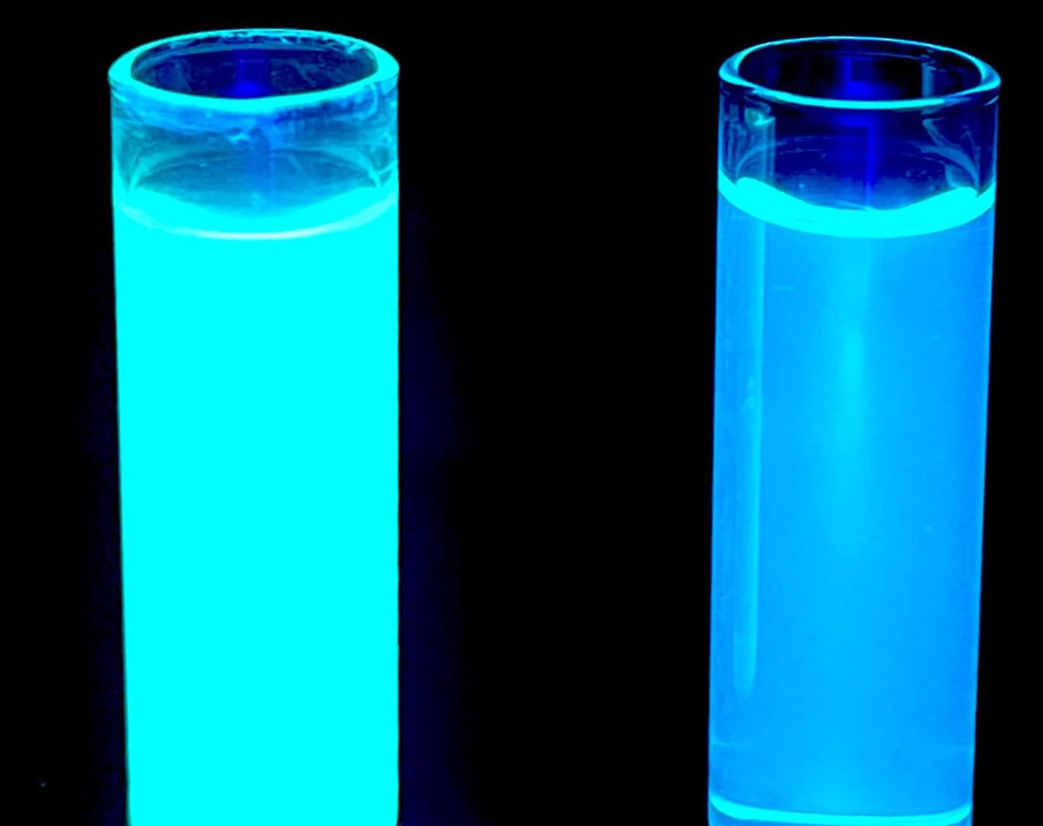
University of Missouri researchers developed the tiny clay-based materials that can be customized for a range of analytical, commercial and medical applications.
Imagine tiny LEGO pieces that automatically snap together to form a strong, flat sheet. Then, scientists add special chemical “hooks” to these sheets to attach glowing molecules called fluorophores.
Associate Professor Gary Baker, Piyuni Ishtaweera, Ph.D., and their team have created these tiny, clay-based materials—called fluorescent polyionic nanoclays. They can be customized for many uses, including advancing energy and sensor technology, improving medical treatments and protecting the environment.

What if there were a fabric that, like Superman, could take a bullet and self-heal? Such a super-dynamic, action-powered polymer might actually help protect real-life flyers in space.
Material scientists at Texas A&M University have developed just such a polymer with a unique self-healing property never before seen at any scale. When struck by a projectile, this material stretches so much that when the projectile manages to pass through, it takes only a small amount of the polymer with it. As a result, the hole left behind is much smaller than the projectile itself.
However, for now, this effect has only been observed under extreme temperatures and at the nanoscale.
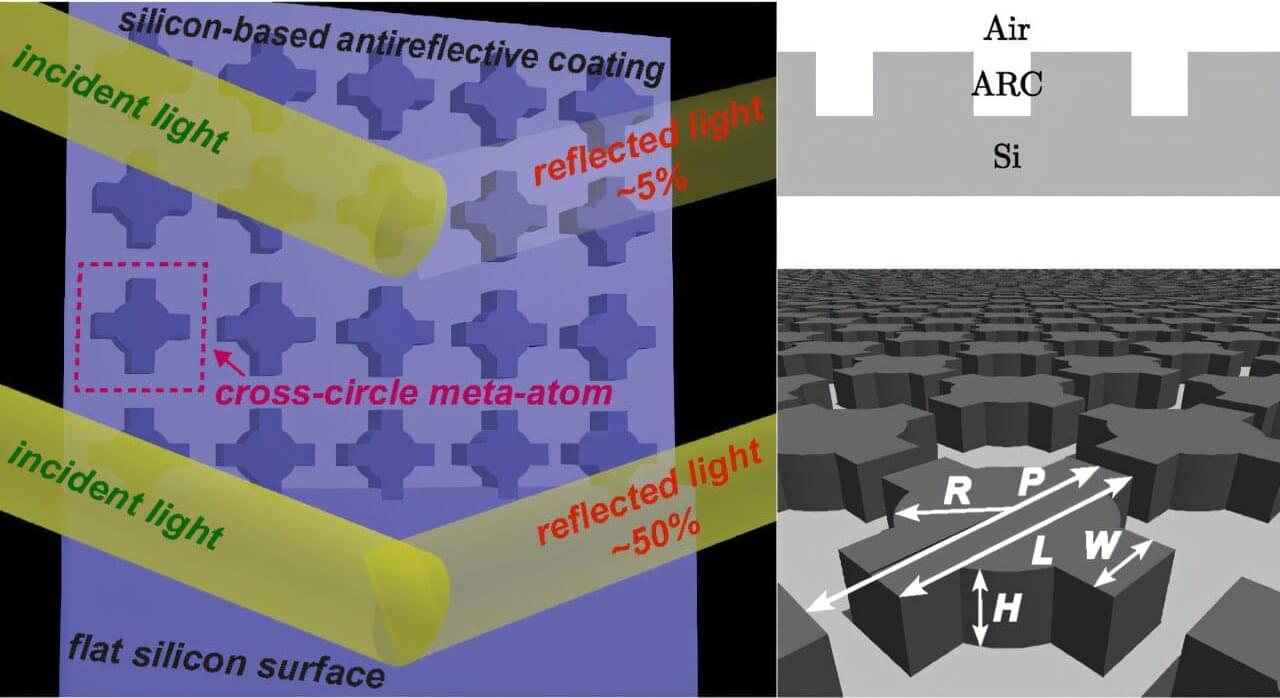
Converting sunlight into electricity is the task of photovoltaic solar cells, but nearly half the light that reaches a flat silicon solar cell surface is lost to reflection. While traditional antireflective coatings help, they only work within a narrow range of light frequency and incidence angles. A new study may have overcome this limit.
As reported in Advanced Photonics Nexus, researchers have proposed a new type of antireflective coating using a single, ultrathin layer of polycrystalline silicon nanostructures (a.k.a. a metasurface). Achieving minimal reflection across certain wavelengths and angles, the metasurface was reportedly developed by combining forward and inverse design techniques, enhanced by artificial intelligence (AI).
The result is a coating that sharply reduces sunlight reflection across a wide range of wavelengths and angles, setting a new benchmark for performance with minimal material complexity.

Researchers at Swansea University have discovered a way to use mirrors to dramatically reduce the quantum noise that disturbs tiny particles—a breakthrough that might seem magical but is rooted in quantum physics.
When scientists measure extremely small objects, such as nanoparticles, they face a difficult challenge: simply observing these particles disturbs them. This happens because photons, particles of light, used for measurement “kick” the tiny particles they hit, an effect known as “backaction.”
In a new study published in Physical Review Research, a team from the university’s Physics Department has revealed a remarkable connection, that this relationship works both ways.
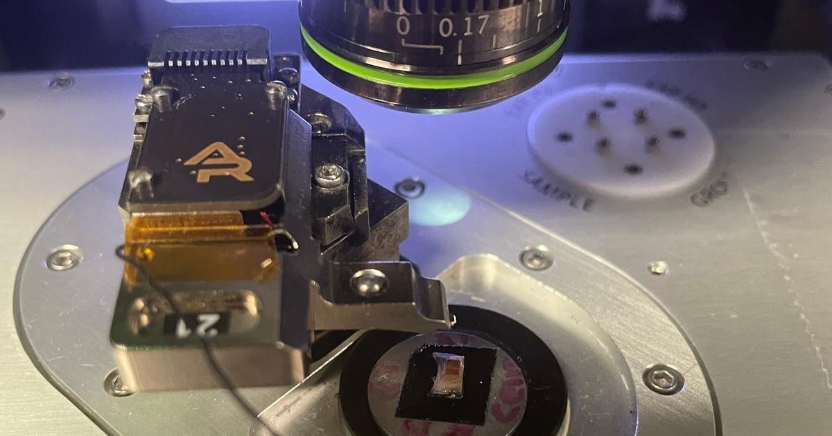
Although lumber does show promise as a renewable alternative to structural materials such as steel and concrete, it still tends to be a bit weaker than those substances. Scientists have now set about addressing that shortcoming, by strengthening wood with added iron.
Led by Asst. Prof. Vivian Merk, a team of researchers at Florida Atlantic University (FAU) started out with cubes of untreated red oak hardwood. Red oak – along with hardwoods like maple, cherry and walnut – is an example of what’s known as ring-porous wood. In a nutshell, this means that it utilizes large ring-shaped internal vessels to draw water up from the tree’s roots to its leaves.
The scientists proceeded to mix ferric nitrate with potassium hydroxide, creating a hard iron oxide mineral called nanocrystalline ferrihydrite, which occurs naturally in soil and water. Utilizing a vacuum impregnation process, nanoparticles of that ferrihydrite were drawn into the wood and deposited inside of its individual cell walls.
Alkali and alkaline earth metal hydrides hold great promise for hydrogen storage and hydrogen-involved chemical transformations due to the unique properties of hydridic hydrogen (H-). However, bulk hydrides often suffer from high lattice energy and limited exposure of active sites, hindering their catalytic performance.
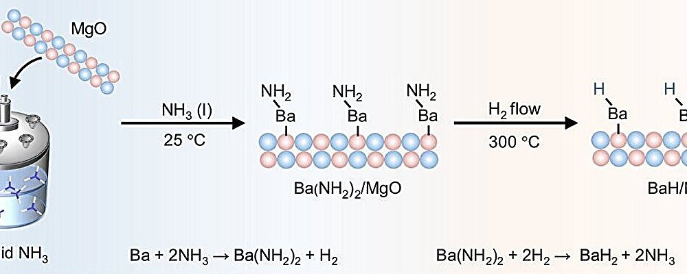
In a study published in Nature Communications, a research group led by Prof. Guo Jianping and Prof. Chen Ping from the Dalian Institute of Chemical Physics of the Chinese Academy of Sciences, collaborating with Prof. Chang Fei from Yongjiang Laboratory and Prof. Rao Li, from Central China Normal University, developed atomically dispersed barium hydride catalysts for the synthesis of deuterated alkylarenes.
Researchers synthesized atomically dispersed barium hydride catalysts on magnesium oxide (BaH/MgO) using a convenient impregnation-hydrogenation method. This (sub)nanostructured hydride material acted as an efficient, transition metal-free heterogeneous catalyst for hydrogen activation and hydrogen isotope exchange reactions across a range of nonactivated alkylarene substrates.
Future drops, freebies & digital gifts – Don’t miss out! Join here:
https://docs.google.com/forms/d/e/1FAIpQLSdeuqNNvEjhpL_PQrF4…usp=dialog.
Ray Kurzweil, one of the world’s leading futurists, has made hundreds of predictions about technology’s future. From portable devices and wireless internet to brain-computer interfaces and nanobots in our bloodstream, Kurzweil has envisioned a future that sometimes feels like science fiction—but much of it is becoming reality.
In this video, we explore 7 of Ray Kurzweil’s boldest predictions:
00:00 — 01:44 Intro.
01:44 — 02:42 Prediction 1: Portable Devices and Wireless Internet.
02:42 — 03:34 Prediction 2: Self-Driving Cars by Early 2020s.
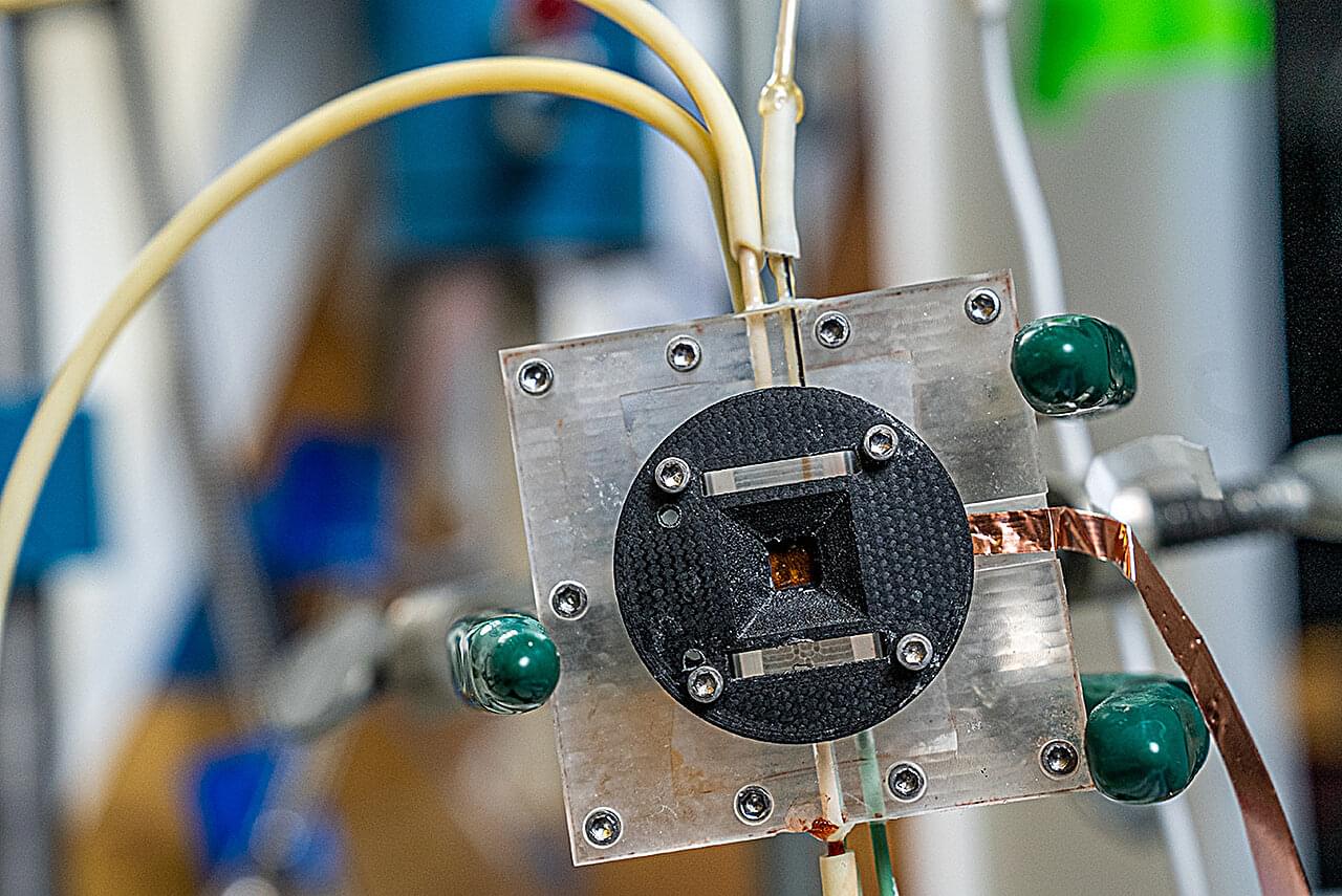
New research has revealed the fundamental mechanisms that limit the performance of copper catalysts—critical components in artificial photosynthesis that transform carbon dioxide and water into valuable fuels and chemicals.
In a study co-led by scientists at Lawrence Berkeley National Laboratory (Berkeley Lab) and SLAC National Accelerator Laboratory, researchers have used sophisticated X-ray techniques to directly observe how copper nanoparticles change during the catalytic process.
By applying small-angle X-ray scattering (SAXS)—a technique traditionally used to study soft materials like polymers—to this catalyst system, the team gained unprecedented insights into catalyst degradation that has puzzled scientists for decades.
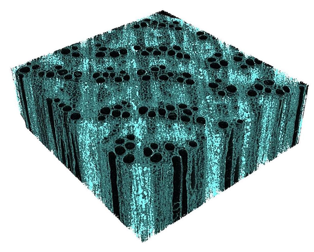
Scientists and engineers are developing high-performance materials from eco-friendly sources like plant waste. A key component, lignocellulose—found in wood and many plants—can be easily collected and chemically modified to improve its properties.
By using these kinds of chemical changes, researchers are creating advanced materials and new ways to design and build sustainably. With about 181.5 billion tons of wood produced globally each year, it’s one of the largest renewable material sources.