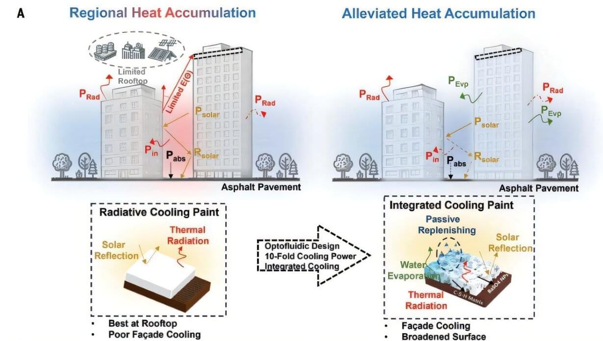
During her uncle’s treatment in 2003, Green experienced what she refers to as a “divine download”—an electrifying idea inspired by her college internships at NASA’s Marshall Space Flight Center and the Institute of Optics. “If a satellite in outer space can tell if a dime on the ground is face up or face down, and if a cell phone can target just one cell phone on the other side of the planet,” she recalls thinking, “surely we should be able to harness the technology of lasers to treat cancer just at the site of the tumor, so we won’t have all of these side effects.”
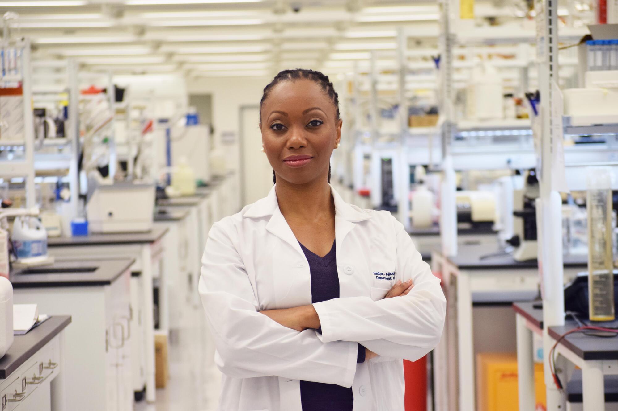
In the nearly two decades that followed, Dr. Green rerouted her career, earned a physics PhD from the University of Alabama at Birmingham—the second Black woman to do so—and dove into cancer treatment research, with physics as her guide. In 2009, she developed a treatment that uses nanoparticles and lasers in tandem: Specially designed nanoparticles are injected into a solid tumor, and, when the tumor is hit with near infrared light, the nanoparticles heat up, killing the cancer cells. In a preliminary animal study published in 2014, Green tested the treatment on mice, whose tumors were eliminated with no observable side effects.
When Hadiyah-Nicole Green crossed the stage at her college graduation, she felt sure about what would come next. She’d start a career in optics—a good option for someone with a bachelor’s degree in physics—and that would be that.
Life, though, had other plans. The day after she graduated from Alabama A&M University, she learned that her aunt, Ora Lee Smith, had cancer. Smith and her husband had raised Green since she was four years old, after the death of Green’s mother and then grandparents.
Her aunt “said she’d rather die than experience the side effects of chemo or radiation,” says Green, now a medical physicist and founder and CEO of the Ora Lee Smith Cancer Research Foundation.