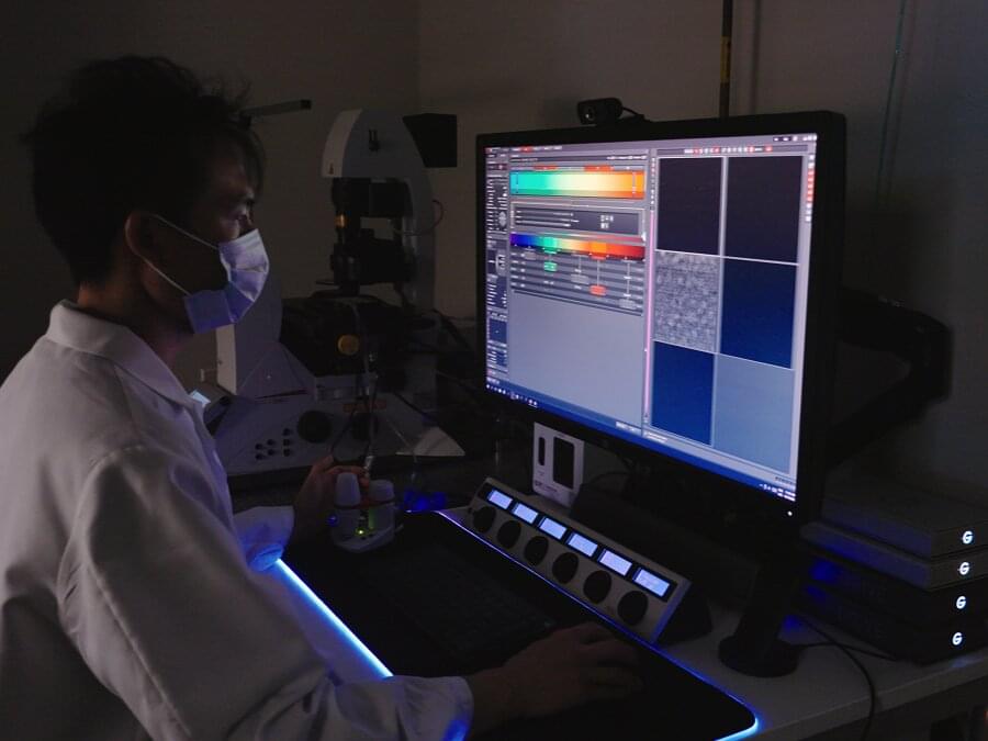
Menu

Blog

Archive for the ‘nanotechnology’ category: Page 189

Jun 18, 2019

A self-assembled nanoscale robotic arm controlled by electric fields

Posted by in categories: biotech/medical, nanotechnology, robotics/AI

Most nanoelectromechanical systems are formed by etching inorganic materials such as silicon. Kopperger et al. improved the precision of such machines by synthesizing a 25-nm-long arm defined by a DNA six-helix bundle connected to a 55 nm-by-55 nm DNA origami plate via flexible single-stranded scaffold crossovers (see the Perspective by Hogberg). When placed in a cross-shaped electrophoretic chamber, the arms could be driven at angular frequencies of up to 25 Hz and positioned to within 2.5 nm. The arm could be used to transport fluorophores and inorganic nanoparticles.

Science, this issue p. 296; see also p. 279

The use of dynamic, self-assembled DNA nanostructures in the context of nanorobotics requires fast and reliable actuation mechanisms. We therefore created a 55-nanometer–by–55-nanometer DNA-based molecular platform with an integrated robotic arm of length 25 nanometers, which can be extended to more than 400 nanometers and actuated with externally applied electrical fields. Precise, computer-controlled switching of the arm between arbitrary positions on the platform can be achieved within milliseconds, as demonstrated with single-pair Förster resonance energy transfer experiments and fluorescence microscopy. The arm can be used for electrically driven transport of molecules or nanoparticles over tens of nanometers, which is useful for the control of photonic and plasmonic processes. Application of piconewton forces by the robot arm is demonstrated in force-induced DNA duplex melting experiments.

Jun 17, 2019

New quantum dot microscope shows electric potentials of individual atoms

Posted by in categories: computing, nanotechnology, particle physics, quantum physics

A team of researchers from Jülich in cooperation with the University of Magdeburg has developed a new method to measure the electric potentials of a sample at atomic accuracy. Using conventional methods, it was virtually impossible until now to quantitatively record the electric potentials that occur in the immediate vicinity of individual molecules or atoms. The new scanning quantum dot microscopy method, which was recently presented in the journal Nature Materials by scientists from Forschungszentrum Jülich together with partners from two other institutions, could open up new opportunities for chip manufacture or the characterization of biomolecules such as DNA.

The positive atomic nuclei and negative electrons of which all matter consists produce electric potential fields that superpose and compensate each other, even over very short distances. Conventional methods do not permit quantitative measurements of these small-area fields, which are responsible for many material properties and functions on the nanoscale. Almost all established methods capable of imaging such potentials are based on the measurement of forces that are caused by electric charges. Yet these forces are difficult to distinguish from other forces that occur on the nanoscale, which prevents quantitative measurements.

Four years ago, however, scientists from Forschungszentrum Jülich discovered a method based on a completely different principle. Scanning quantum dot microscopy involves attaching a single organic molecule—the quantum dot—to the tip of an atomic microscope. This molecule then serves as a probe. “The molecule is so small that we can attach individual electrons from the tip of the atomic force microscope to the molecule in a controlled manner,” explains Dr. Christian Wagner, head of the Controlled Mechanical Manipulation of Molecules group at Jülich’s Peter Grünberg Institute (PGI-3).

Jun 16, 2019

Self-cleaning Clothes Made Possible By Nano-enhanced Textile

Posted by in categories: energy, nanotechnology

Circa 2016


Not a big fan of laundry day? Well what if you could wash your clothes just by stepping into the sunshine? Thanks to researchers at RMIT University in Melbourne, a self-cleaning textile could make that possible in the very near future. With the help of special nanostructures grown directly into the fabric, these new textiles could degrade organic matter like dirt, dust, and sweat when exposed to a concentrated light source.

To achieve this effect, the nanostructures used by the RMIT University team are made copper and silver. These metals are great at absorbing visible light, and when they’re exposed to light from the sun or even a light bulb, the nanostructures react with increased energy that creates “hot electrons”.

Continue reading “Self-cleaning Clothes Made Possible By Nano-enhanced Textile” »

Jun 15, 2019

Conjugating Carboxylic Acid Functionalized Gold Nanoparticles

Posted by in category: nanotechnology

Conjugating Carboxylic Acid Functionalized Gold Nanoparticles, unlike other gold nanoparticles, are pre-ready for covalent conjugation. The carboxlic acid groups on the surface of the gold nanoparticles are easily reacted with primary amines via a condensation reaction which yields strong amide bonds. Usually, this is achieved by using a water-soluble carbodiimide linker such as EDC.

https://nanohybrids.net/pages/conjugating-carboxyl-functiona…oparticles

⬇️

Jun 15, 2019

Nanoscale optical imaging gets simpler and cheaper

Posted by in category: nanotechnology

With a lens-free makeover scanning near-field optical microscopes (SNOMs) could become a common lab tool.

Jun 11, 2019

Engineers design nanostructured diamond metalens for compact quantum technologies

Posted by in categories: computing, nanotechnology, particle physics, quantum physics

At the chemical level, diamonds are no more than carbon atoms aligned in a precise, three-dimensional (3D) crystal lattice. However, even a seemingly flawless diamond contains defects: spots in that lattice where a carbon atom is missing or has been replaced by something else. Some of these defects are highly desirable; they trap individual electrons that can absorb or emit light, causing the various colors found in diamond gemstones and, more importantly, creating a platform for diverse quantum technologies for advanced computing, secure communication and precision sensing.

Quantum technologies are based on units of quantum information known as “qubits.” The spin of electrons are prime candidates to serve as qubits; unlike binary computing systems where data takes the form of only 0s or 1s, electron spin can represent information as 0, 1, or both simultaneously in a quantum superposition. Qubits from are of particular interest to quantum scientists because their quantum-mechanical properties, including superposition, exist at room temperature, unlike many other potential quantum resources.

The practical challenge of collecting information from a single atom deep inside a crystal is a daunting one, however. Penn Engineers addressed this problem in a recent study in which they devised a way to pattern the surface of a diamond that makes it easier to collect light from the defects inside. Called a metalens, this contains nanoscale features that bend and focus the light emitted by the defects, despite being effectively flat.

Continue reading “Engineers design nanostructured diamond metalens for compact quantum technologies” »

Jun 10, 2019

Researchers find a way to make Casimir effect attract or repulse depending on gap size

Posted by in categories: nanotechnology, quantum physics

A team of researchers from the University of California at Berkeley and Lawrence Berkeley National Laboratory has found a way to make the Casimir effect attract or repulse depending on the size of the gap between two objects. In their paper published in the journal Science, the group describes their technique and possible applications.

The Casimir effect, first proposed by Hendrik Casimir back in 1948, is the phenomenon in which two tiny surfaces in close proximity experience a force that pulls them closer together. Quantum fluctuations inside and outside of the gap push against the plates, but because those pushing from the outside are stronger, they create an between the two plates. The Casimir effect is more than a curiosity, because it can create problems in nanotechnology applications.

Just two years after Casimir first proposed the effect, others in the field began making predictions about ways to counter it—making it repulsive rather than attractive, for example, in the case of fluids and plates made of lower refractive metals. Then, in 2010, a team at MIT suggested that it should be possible to counter both attractive and repulsive effects to create a state of equilibrium between the two plates. In this new effort, the researchers report that they have done just that.

Continue reading “Researchers find a way to make Casimir effect attract or repulse depending on gap size” »

Jun 10, 2019

Fiber-optic probe can see molecular bonds

Posted by in categories: engineering, nanotechnology, quantum physics

In “Avengers: Endgame,” Tony Stark warned Scott Lang that sending him into the quantum realm and bringing him back would be a “billion-to-one cosmic fluke.”

In reality, shrinking a to a nanometer-sized point to spy on quantum-scale -matter interactions and retrieving the information is not any easier. Now, engineers at the University of California, Riverside, have developed a new technology to tunnel light into the quantum realm at an unprecedented efficiency.

In a Nature Photonics paper, a team led by Ruoxue Yan, an assistant professor of chemical and , and Ming Liu, an assistant professor of electrical and computer engineering, describe the world’s first portable, inexpensive, optical nanoscopy tool that integrates a glass optical fiber with a silver nanowire condenser. The device is a high-efficiency round-trip light tunnel that squeezes visible light to the very tip of the condenser to interact with molecules locally and send back information that can decipher and visualize the elusive nanoworld.

Continue reading “Fiber-optic probe can see molecular bonds” »

Jun 10, 2019

Laser-driven Particle Accelerator Made Ten Thousand Times Smaller

Posted by in categories: biotech/medical, computing, nanotechnology

Dielectric laser accelerators (DLAs) provide a compact and cost-effective solution to this problem by driving accelerator nanostructures with visible or near-infrared (NIR) pulsed lasers, resulting in a 10,000 times reduction of scale. Current implementations of DLAs rely on free-space lasers directly incident on the accelerating structures, limiting the scalability and integrability of this technology. Researchers present the first experimental demonstration of a waveguide-integrated DLA, designed using a photonic inverse design approach. These on-chip devices accelerate sub-relativistic electrons of initial energy 83.4 keV by 1.21 keV over 30 µm, providing peak acceleration gradients of 40.3 MeV/m. This progress represents a significant step towards a completely integrated MeV-scale dielectric laser accelerator.

Dielectric laser accelerators have emerged as a promising alternative to conventional RF accelerators due to the large damage threshold of dielectric materials the commercial availability of powerful NIR femtosecond pulsed lasers, and the low-cost high-yield nanofabrication processes which produce them. Together, these advantages allow DLAs to make an impact in the development of applications such as tabletop free-electron-lasers, targeted cancer therapies, and compact imaging sources.

They have designed and experimentally verified the first waveguide-integrated DLA structure. The design of this structure was made possible through the use of photonics inverse design methodologies developed by the team members. The fabricated and experimentally demonstrated devices accelerate electrons of an initial energy of 83.4 keV by a maximum energy gain of 1.21 keV over 30 µm, demonstrating acceleration gradients of 40.3 MeV/m. In this integrated form, these devices can be cascaded to reach MeV-scale energies, capitalizing on the inherent scalability of photonic circuits. Future work will focus on multi-stage demonstrations, as well as exploring new design and material solutions to obtain larger gradients.

Continue reading “Laser-driven Particle Accelerator Made Ten Thousand Times Smaller” »

Jun 10, 2019

A Thousand Times Better Instrument Will Investigate Emdrive and Mach Propulsion

Posted by in categories: nanotechnology, quantum physics

Martin Tajmar has a SpaceDrive project and plans to create an instrument so sensitive and immune to interference that it would put an end to the debate once and for all. Tajmar believes that studying the EmDrive and similar propellantless propulsion systems will requir nano-newton instrument resolution.

He is making a new to torsion balance. It is a pendulum-type balance that measures the amount of torque applied to the axis of the pendulum. Tajmar’s team used a laser interferometer to measure the physical displacement of the balance scales. The new torsion scale has a nano-newton resolution and supports thrusters weighing several pounds, making it the most sensitive thrust balance in existence.

The SpaceDrive Project-Thrust Balance Development and New Measurements of the Mach-Effect and EMDrive Thrusters.

Continue reading “A Thousand Times Better Instrument Will Investigate Emdrive and Mach Propulsion” »