Toggle light / dark theme

Graphene, an atomically thin carbon layer through which electrons can travel virtually unimpeded, has been extensively studied since its first successful isolation more than 15 years ago. Among its many unique properties is the ability to support highly confined electromagnetic waves coupled to oscillations of electronic charge—plasmon polaritons—that have potentially broad applications in nanotechnology, including biosensing, quantum information, and solar energy.

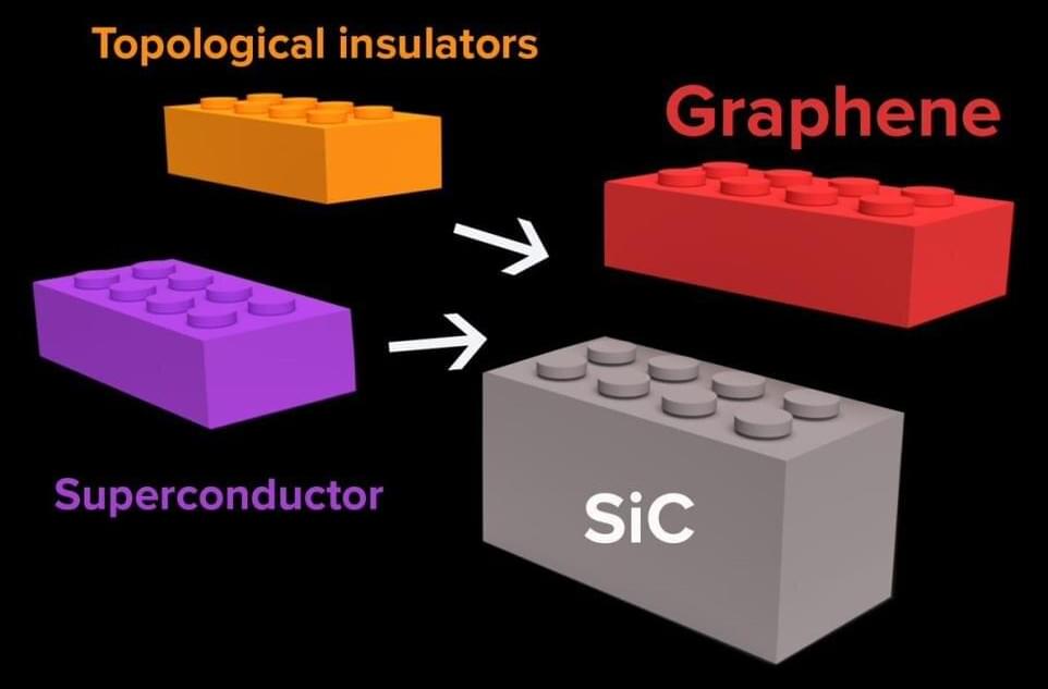
However, in order to support , must be charged by applying a voltage to a nearby metal gate, which greatly increases the size and complexity of nanoscale devices. Columbia University researchers report that they have achieved plasmonically active graphene with record-high charge density without an external gate. They accomplished this by exploiting novel interlayer charge transfer with a two-dimensional electron-acceptor known as α-RuCl3. The study is available now online as an open access article and will appear in the December 9th issue of Nano Letters.

“This work allows us to use graphene as a plasmonic material without metal gates or voltage sources, making it possible to create stand-alone graphene plasmonic structures for the first time” said co-PI James Hone, Wang Fong-Jen Professor of Mechanical Engineering at Columbia Engineering.

“The newest term — Universal Basic Means of Production — helps someone unfamiliar with the concepts to better imagine that world without clouding the idea with negative connotations from the past. So, what if instead of focusing so heavily on the idea of passing out money to individuals, we shift our focus to subsidizing 3D printers, local recycling centers for collecting plastic to make 3D printing filament when possible, and vertical gardens in homes and communities.”


Imagine a carbon nanotube replicator and garden in every home. It’s not sci-fi and will soon be possible. How fast we make the transition is entirely up to us.

This term refers to the idea of providing every household with technology that allows people to produce things they need at home. This includes consumer goods such as clothes, food, building materials, etc. and refers to the idea of getting everyone producing as many of their consumable materials as possible.

In many ways, we can think of it as creating a decentralized means of production, although it’s not entirely decentralized. And when you get right down to it, the whole point of a decentralized means of production is people working together to produce things they need. Not just some corporate “shareholder value” conference.

There are several ways to generate power from that mixing. And a couple of blue energy power plants have been built. But their high cost has prevented widespread adoption. All blue energy approaches rely on the fact that salts are composed of ions, or chemicals that harbor a positive or negative charge. In solids, the positive and negative charges attract one another, binding the ions together. (Table salt, for example, is a compound made from positively charged sodium ions bound to negatively charged chloride ions.) In water, these ions detach and can move independently.

By pumping the positive ions—like sodium or potassium—to the other side of a semipermeable membrane, researchers can create two pools of water: one with a positive charge, and one with a negative charge. If they then dunk electrodes in the pools and connect them with a wire, electrons will flow from the negatively charged to the positively charged side, generating electricity.

In 2013, French researchers made just such a membrane. They used a ceramic film of silicon nitride—commonly used in industry for electronics, cutting tools, and other uses—pierced by a single pore lined with a boron nitride nanotube (BNNT), a material being investigated for use in high-strength composites, among other things. Because BNNTs are highly negatively charged, the French team suspected they would prevent negatively charged ions in water from passing through the membrane (because similar electric charges repel one another). Their hunch was right. They found that when a membrane with a single BNNT was placed between fresh- and saltwater, the positive ions zipped from the salty side to the fresh side, but the negatively charged ions were mostly blocked.

Scientists at Osaka University develop a label-free method for identifying respiratory viruses based on changes in electrical current when they pass through silicon nanopores, which may lead to new rapid COVID-19 tests.

The ongoing global pandemic has created an urgent need for rapid tests that can diagnose the presence of the SARS-CoV-2 virus, the pathogen that causes COVID-19, and distinguish it from other respiratory viruses. Now, researchers from Japan have demonstrated a new system for single-virion identification of common respiratory pathogens using a machine learning algorithm trained on changes in current across silicon nanopores. This work may lead to fast and accurate screening tests for diseases like COVID-19 and influenza.

In a study published this month in ACS Sensors scientists at Osaka University have introduced a new system using silicon nanopores sensitive enough to detect even a single virus particle when coupled with a machine learning algorithm.

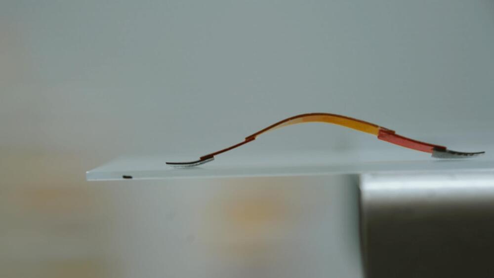
A material that mimics human skin in strength, stretchability and sensitivity could be used to collect biological data in real time. Electronic skin, or e-skin, may play an important role in next-generation prosthetics, personalized medicine, soft robotics and artificial intelligence.

“The ideal e-skin will mimic the many natural functions of human skin, such as sensing temperature and touch, accurately and in real time,” says KAUST postdoc Yichen Cai. However, making suitably flexible electronics that can perform such delicate tasks while also enduring the bumps and scrapes of everyday life is challenging, and each material involved must be carefully engineered.

Most e-skins are made by layering an active nanomaterial (the sensor) on a stretchy surface that attaches to human skin. However, the connection between these layers is often too weak, which reduces the durability and sensitivity of the material; alternatively, if it is too strong, flexibility becomes limited, making it more likely to crack and break the circuit.

An international team of scientist from the United States, the United Kingdom and Taiwan has developed the world’s smallest memristor. Their results appear in the journal Nature Nanotechnology.

In the new work, the researchers reduced the size even further, shrinking the cross section area down to just a single square nanometer.

What if with the new wave of technologies, such as nanotechnology which would enable us to reprogram matter at a molecular level, we can overcome scarcity once and for all? Design would then become the most important part from start to end product which can be freely shared or have a premium in the marketplace. At any rate, this will dismantle the current social, economic, and political system, because it will become irrelevant; every institution, every value system, every aspect of our lives have been governed by scarcity: the problem of distributing a finite amount of “stuff.” There will be no need for any of today’s social institutions. In other words, when nanotech and ultra-realistic VR are commonplace, the system built on scarcity will crumble and that would herald the forthcoming “economic singularity.” #EconomicSiingularity


The current faltering economic model is suboptimal, hinders economic growth, and is not sustainable going forward.

When light falls on a material, such as a green leaf or the retina, certain molecules transport energy and charge. This ultimately leads to the separation of charges and the generation of electricity. Molecular funnels, so-called conical intersections, ensure that this transport is highly efficient and directed.

An international team of physicists has now observed that such conical intersections also ensure a directed energy transport between neighboring of a nanomaterial. Theoretical simulations have confirmed the . Until now, scientists had observed this phenomenon only within one molecule. In the long term, the results could help to develop more efficient nanomaterials for organic solar cells, for example. The study, led by Antonietta De Sio, University of Oldenburg, and Thomas Frauenheim, University of Bremen, Germany, was published in the current issue of the scientific journal Nature Nanotechnology.

Photochemical processes play a major role in nature and in technology: When molecules absorb light, their electrons transit to an excited state. This transition triggers extremely fast molecular switching processes. In the human eye, for example, the molecule rhodopsin rotates in a certain way after absorbing light and thus ultimately triggers an electrical signal—the most elementary step in the visual process.

The work was conducted in the laboratory of Dan Peer, PhD, VP for R&D and Head of the Laboratory of Precision Nanomedicine at the Shmunis School of Biomedicine and Cancer Research at TAU. The research was conducted by Daniel Rosenblum, PhD, together with PhD student Anna Gutkin and colleagues in Peer’s laboratory and other collaborators.

The study “CRISPR-Cas9 genome editing using targeted lipid nanoparticles for cancer therapy” appears in Science Advances.

“Harnessing CRISPR-Cas9 technology for cancer therapeutics has been hampered by low editing efficiency in tumors and potential toxicity of existing delivery systems. Here, we describe a safe and efficient lipid nanoparticle (LNP) for the delivery of Cas9 mRNA and sgRNAs that use a novel amino-ionizable lipid,” write the investigators.