Ago when I was a kid in college my friend Eric got me into many things. We played music together and used a Kurzweil Keyboard, and a bunch of weird stuff. We had an ADAT hooked up to the Kurzweil with fiber optic cables. I had Roland keyboards & Drum machines but I loved the Kurzweil. He started teaching me many things because he was really smart. I was studying psychology so he loaned me his DSMIV and books on Industrial Organiza… See more.
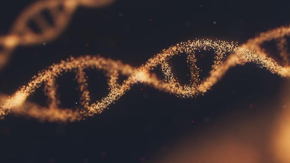
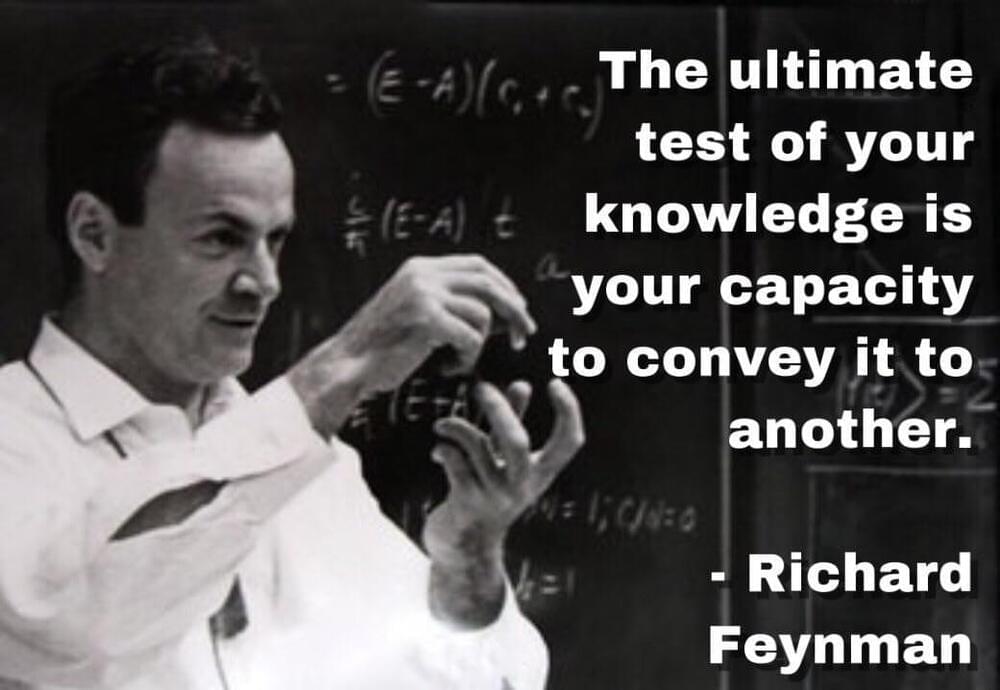
A bit long, but a good read. About 20 years ago when I was a kid in college my friend Eric got me into many things. We played music together and used a Kurzweil Keyboard, and a bunch of weird stuff. We had an ADAT hooked up to the Kurzweil with fiber optic cables. I had Roland keyboards & Drum machines but I loved the Kurzweil. He started teaching me many things because he was really smart. I was studying psychology so he loaned me his DSMIV and books on Industrial Organizational Psychology. He then told me about other books like “Society of Mind”(Marvin Minsky), “Age of Intelligent Machine” (Ray Kurzweil), Engines of Creation (K Eric Drexler), of course Richard Feynman, and many more. I dreamed of that technology and kept reading more. In the 2000’s Drexler and Feynman’s visions became a paradign and applications started rolling out, and now nanotechnology is applied to most everything we know. We are now at the second paradigm where we see the visions of Minsky/McCarthy, Kurzweil and others becoming easily available applications. As a Child I watched the Jetsons & Srar Trek and now with flying cars it’s not if, but when. Space travel is already here. All these technologies will transform global societies, but we must all focus on investing more in the advancement of society than the destruction of it. Many of the things we now invision in our minds we may see in 10 years. People think saving your consciousness & longevity is impossible, but I don’t. Some even thought that regenerating tissue and organs is impossible, but we can do that now. Now people keep saying, “This ancient turtle died, this rhino died (I hear that all the time in Kenya), this elephant died, but I say okay it’s not cool, but what can we salvage from it to bring the species back with advances in technology later? Do we use cryogenics? How do we save the genetic material? Technology can be used in so many ways. Every Day Lifeboat posts feats many do not know. If more people on earth had such a focus, as opposed to dumbed down entertainment like The Kardashians for instance, we would be living in a much better world with more people proposing more ideas and collaborations. I always say we are moving in the wrong way in the evolutionary process, and it is a bit telling that some phones are smarter than many people. I you add ChatGPT. We have so much advanced technology and science, yet we can’t even fight cancer. It took decades for people to learn the importance of diet in HIV treatment. However, Ray Kurzweil has for decades talked about the importance of diet for longevity. Just the other day it was published that processed foods affect cognitive function. Before that it was released processed foods cause cancer. We must change, and go in the right way of evolution to the Singularity another paradigm shift and cooperarion, instead of backwards to a barbaric age of conflict and greed. Always share your knowledge and I thank all who do share in this group. More should share as well, and Lifeboat should use more platforms to reach more people.