Toggle light / dark theme

Circa 2020 Basically this means a magnetic transistor can have not only quantum properties but also it can have nearly infinite speeds for processing speeds. Which means we can have nanomachines with near infinite speeds eventually.


Abstract The discovery of spin superfluidity in antiferromagnetic superfluid 3He is a remarkable discovery associated with the name of Andrey Stanislavovich Borovik-Romanov. After 30 years, quantum effects in a magnon gas (such as the magnon Bose–Einstein condensate and spin superfluidity) have become quite topical. We consider analogies between spin superfluidity and superconductivity. The results of quantum calculations using a 53-bit programmable superconducting processor have been published quite recently[1]. These results demonstrate the advantage of using the quantum algorithm of calculations with this processor over the classical algorithm for some types of calculations. We consider the possibility of constructing an analogous (in many respecys) processor based on spin superfluidity.

9 nov 2022.


The challenge of fabricating nanowires directly on silicon substrates for the creation of the next generation of electronics has finally been solved by researchers from Tokyo Tech. Next-generation spintronics will lead to better memory storage mechanisms in computers, making them faster and more efficient.

As our world modernizes faster than ever before, there is an ever-growing need for better and faster electronics and computers. Spintronics is a new system which uses the spin of an electron, in addition to the charge state, to encode data, making the entire system faster and more efficient. Ferromagnetic nanowires with high coercivity (resistance to changes in magnetization) are required to realize the potential of spintronics. Especially L 10-ordered (a type of crystal structure) cobalt-platinum (CoPt) nanowires.

Conventional fabrication processes for L 10-ordered nanowires involve heat treatment to improve the physical and chemical properties of the material, a process called annealing on the crystal substrate; the transfer of a pattern onto the substrate through lithography; and finally the chemical removal of layers through a process called etching. Eliminating the etching process by directly fabricating nanowires onto the silicon substrate would lead to a marked improvement in the fabrication of spintronic devices. However, when directly fabricated nanowires are subjected to annealing, they tend to transform into droplets as a result of the internal stresses in the wire.

A new technology developed at Tel Aviv University makes it possible to destroy cancerous tumors in a targeted manner, via a combination of ultrasound and the injection of nanobubbles into the bloodstream. According to the research team, unlike invasive treatment methods or the injection of microbubbles into the tumor itself, this latest technology enables the destruction of the tumor in a non-invasive manner.

The study was conducted under the leadership of doctoral student Mike Bismuth from the lab of Dr. Tali Ilovitsh at Tel Aviv University’s Department of Biomedical Engineering, in collaboration with Dr. Dov Hershkovitz of the Department of Pathology. Prof. Agata Exner from Case Western Reserve University in Cleveland also participated in the study. The study was published in the journal Nanoscale.

Dr. Tali Ilovitsh says that their “new technology makes it possible, in a relatively simple way, to inject nanobubbles into the bloodstream, which then congregate in the area of the cancerous . After that, using a low-frequency ultrasound, we explode the nanobubbles, and thereby the tumor.”

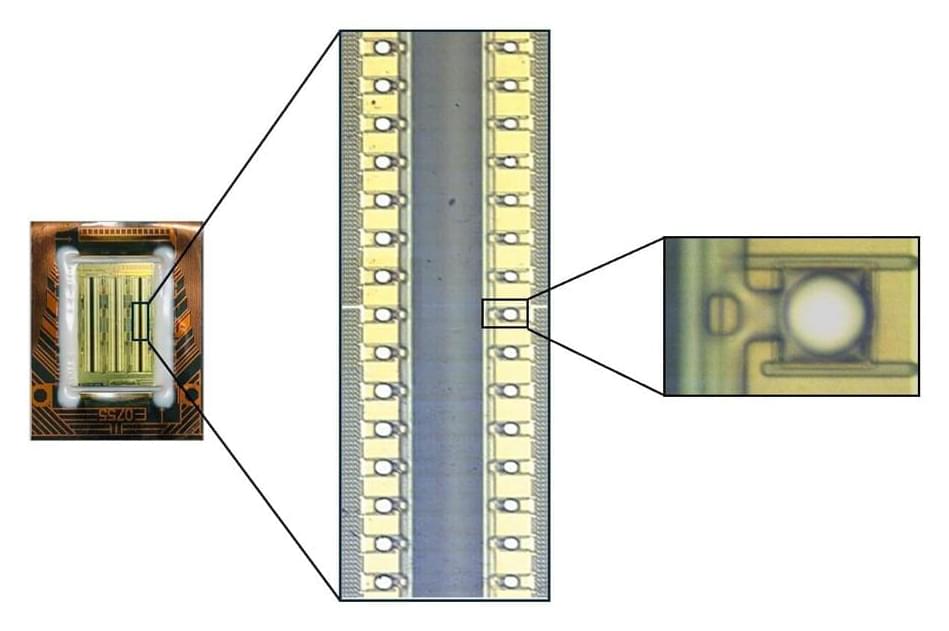
A team of German and Spanish researchers from Valencia, Münster, Augsburg, Berlin and Munich have succeeded in controlling individual light quanta to an extremely high degree of precision. In Nature Communications, the researchers report how, by means of a soundwave, they switch individual photons on a chip back and forth between two outputs at gigahertz frequencies. This method, demonstrated here for the first time, can now be used for acoustic quantum technologies or complex integrated photonic networks.

Light waves and soundwaves form the technological backbone of modern communications. While glass fibers with laser light form the World Wide Web, nanoscale soundwaves on chips process signals at gigahertz frequencies for wireless transmission between smartphones, tablets or laptops. One of the most pressing questions for the future is how these technologies can be extended to , to build up secure (i.e., tap-free) quantum communication networks.

“Light quanta or photons play a very central role in the development of quantum technologies,” says physicist Prof. Hubert Krenner, who heads the study in Münster and Augsburg. “Our team has now succeeded in generating on a chip the size of a thumbnail and then controlling them with unprecedented precision, precisely clocked by means of soundwaves,” he says.

Circa 2020 face_with_colon_three


UNSW researchers have overcome a major design challenge on the path to controlling the dimensions of so-called DNA nanobots—structures that assemble themselves from DNA components.

Self-assembling nanorobots may sound like science fiction, but new research in DNA nanotechnology has brought them a step closer to reality. Future nanobot use cases won’t just play out on the tiny scale, but include larger applications in the health and , such as wound healing and unclogging of arteries.

Circa 2020 face_with_colon_three


Light-activated molecular nanomachines (MNMs) can be used to drill holes into prokaryotic (bacterial) cell walls and the membrane of eukaryotic cells, including mammalian cancer cells, by their fast rotational movement, leading to cell death. We examined how these MNMs function in multicellular organisms and investigated their use for treatment and eradication of specific diseases by causing damage to certain tissues and small organisms. Three model eukaryotic species, Caenorhabditis elegans, Daphnia pulex, and Mus musculus (mouse), were evaluated. These organisms were exposed to light-activated fast-rotating MNMs and their physiological and pathological changes were studied in detail. Slow rotating MNMs were used to control for the effects of rotation rate. We demonstrate that fast-rotating MNMs caused depigmentation and 70% mortality in C.

It’s all thanks to nanoclusters.

A new nanoscale 3D printing material developed by Stanford University engineers may provide superior structural protection for satellites, drones, and microelectronics.


A dual-phase, nanostructured high-entropy alloy that has been 3D printed by researchers from the University of Massachusetts Amherst and the Georgia Institute of Technology is stronger and more ductile than other cutting-edge additively manufactured materials. This discovery could lead to higher-performance components for use in aerospace, medicine, energy, and transportation.

High entropy alloys (HEAs), as they are called, have gained popularity as a new paradigm in materials science over the past 15 years. They allow for the creation of a nearly limitless number of different alloy designs since they include five or more elements in nearly equal amounts. Brass, carbon steel, stainless steel, and bronze are examples of traditional alloys that mix a principal element with one or more trace elements.

In a recently published paper in Nature Electronics, an international research group from Italy, Germany, the UK, and China examined significant development directions in the field of electronic materials with curved geometries at the nanoscale. From microelectronic devices with enhanced functionality to large-scale nanomembranes consisting of networks of electronic sensors that can provide improved performance.

The scientists argue that exciting developments induced by curvature at the nanoscale allow them to define a completely new field—curved nanoelectronics. The paper examines in detail the origin of curvature effects at the and illustrates their potential applications in innovative electronic, spintronic and superconducting devices.

Curved solid-state structures also offer many application opportunities. On a , shape deformations in electronic nanochannels give rise to complex three-dimensional spin textures with an unbound potential for new concepts in spin-orbitronics, which will help develop energy-efficient electronic devices.

At the nanoscale, the laws of classical physics suddenly become inadequate to explain the behavior of matter. It is precisely at this juncture that quantum theory comes into play, effectively describing the physical phenomena characteristic of the atomic and subatomic world. Thanks to the different behavior of matter on these length and energy scales, it is possible to develop new materials, devices and technologies based on quantum effects, which could yield a real quantum revolution that promises to innovate areas such as cryptography, telecommunications and computation.

The physics of very small objects, already at the basis of many technologies that we use today, is intrinsically linked to the world of nanotechnologies, the branch of applied science dealing with the control of matter at the nanometer scale (a nanometer is one billionth of a meter). This control of matter at the is at the basis of the development of new electronic devices.

Among these, are considered promising devices for the realization of new computational architectures emulating functions of our brain, allowing the creation of increasingly efficient computation systems suitable for the development of the entire artificial intelligence sector, as recently shown by Istituto Nazionale di Ricerca Metrologica (INRiM) researchers in collaboration with several international universities and research institutes.