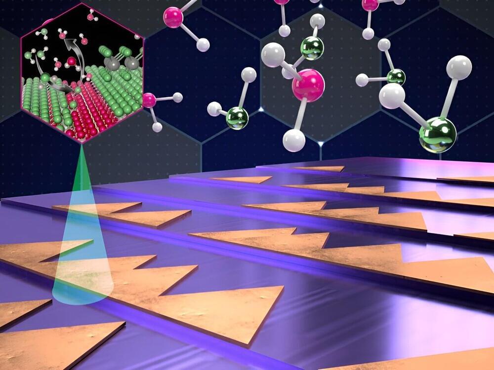
The next generation of 2D semiconductor materials doesn’t like what it sees when it looks in the mirror. Current synthesizing approaches to make single-layer nanosheets of semiconducting material for atomically thin electronics develop a peculiar “mirror twin” defect when the material is deposited on single-crystal substrates like sapphire. The synthesized nanosheet contains grain boundaries that act as a mirror, with the arrangement of atoms on each side organized in reflected opposition to one another.
This is a problem, according to researchers from the Penn State’s Two-Dimensional Crystal Consortium-Materials Innovation Platform (2DCC-MIP) and their collaborators. Electrons scatter when they hit the boundary, reducing the performance of devices like transistors. This is a bottleneck, the researchers said, for the advancement of next-generation electronics for applications such as Internet of Things and artificial intelligence. But now, the research team may have come up with a solution to correct this defect. They have published their work in Nature Nanotechnology.
This study could have a significant impact on semiconductor research by enabling other researchers to reduce mirror twin defects, according to lead author Joan Redwing, director of 2DCC-MIP, especially as the field has increased attention and funding from the CHIPS and Science Act approved last year. The legislation’s authorization increased funding and other resources to boost America’s efforts to onshore the production and development of semiconductor technology.