Knowledge graphs are a powerful tool for bringing together information from biological databases and linking what is already known about genes, diseases, treatments, molecular pathways and symptoms in a structured network. Until now, they have lacked detailed, individual-level information about how the affected organ actually looks and functions.
The latest research, led by postdoctoral researcher Dr. Khaled Rjoob and group leader Professor Declan O’Regan from the Computational Cardiac Imaging Group at the MRC Laboratory of Medical Sciences, has advanced this technology by adding imaging data to a knowledge graph for the first time. CardioKG provides a detailed view of the heart’s structure and function which dramatically improves the accuracy of predicting which genes are linked to disease and whether existing drugs could treat them.
The work is published in the journal Nature Cardiovascular Research.
Tiny molecules that can think, remember, and learn may be the missing link between electronics and the brain. For more than half a century, researchers have looked for ways to move past silicon by building electronics from molecules. The idea sounded simple and beautiful, but real devices turned
Elon Musk’s brain implant company Neuralink will start “high-volume production” of brain-computer interface devices and move to an entirely automated surgical procedure in 2026, Musk said in a post on the social media platform X on Wednesday.
Einstein never liked the idea that nature is uncertain and he once said “does that mean the Moon is not there when I am not looking at it”. He believed we live in an orderly Universe which is fundamentally rational and that there should always be a reason why thing happen. But there is a way to have the objective Universe of Einstein and the uncertainty of quantum physics and that is by explaining quantum mechanics as the physics of ‘time’ with the future as an emergent property.
In this radical theory the mathematics of quantum mechanics represents the physics of ‘time’ as a physical process with classical physics representing process over a period of time as in Newton’s differential equations. This is a process formed by the spontaneous absorption and emission of light photon energy. This forms a continuous process of energy exchange that forms the ever changing world of our everyday life.
The Universe is a continuum with the future coming into existence photon by photon with each new photon electron coupling or dipole moment. This forms the movement of positive and negative charge with the continuous flow of electromagnetic fields.
Consciousness in the form of electrical activity in the brain is the most advanced part of this process and can therefore comprehend this process as ‘time’. With a past that has gone forever and a future that is always uncertain in the form of a probability function or quantum wave particle function that is explained mathematically by Schrödinger’s wave equation Ψ. Therefore each individual is in the centre of their own reference frame as an interactive part of this process. With their own time line from the past into the future being able to look back in time in all directions at the beauty of the stars! It is this personalization of the brain being in ‘the moment of now’ in the center of its own reference frame that gives us the concept of ‘mind’ with each one of us having our own personal view of the beauty and uncertainty of life.
It is not that there is uncertainty if the Moon is there or not if nobody looks. It is that the physical act of looking will form new light photon oscillations or vibrations relative to the actions of the observer in a continuous flow of cause and effect. The wave particle duality of light is acting like the bits or zeros and ones of a computer. This forms an interactive process continuously forming a blank canvas that we can interact with turning the possible into the actual! Any observation of the Moon will be over a period of time with the wave nature of light explaining diffraction, interference, reflection and refraction. But the particle nature of light the ‘photon’ will only come into existence when the light comes in contact with the lenses and mirrors of the telescope being used. And finally with new photons be formed in the eye of the observer the uncertainty of the observation will be completed using both the wave and particle nature of light!
What we see in our everyday life as an uncertain future is formed by a physical process that at the smallest scale is represented mathematically by Heisenberg’s Uncertainty Principle ∆×∆p×≥h/4π with the Planck constant ħ=h/2π being a constant of action in the dynamics geometry of space and time! This theory takes quantum potential, electrical potential and gravitational potential and combines them into one universal process. That explains why we all have a potential future in our everyday life that is always uncertain. This is done by making the future an emergent property energy ∆E slows the rate that time ∆t flows creating a future relative to the energy and momentum of each object or life form. For in this theory creation is truly in the hand and eye of the beholder with an objective reality in the form of a dynamic interactive process that forms an infinity of possibilities. Please share and subscribe it will help the promotion of this theory!
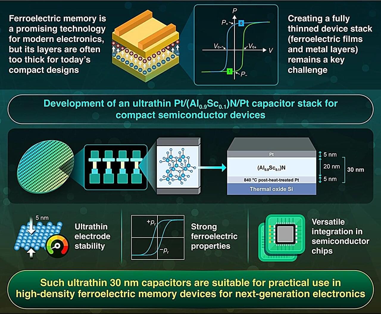
An ultrathin ferroelectric capacitor, designed by researchers from Japan, demonstrates strong electric polarization despite being just 30 nm thick including top and bottom electrodes—making it suitable for high-density electronics. Using a scandium-doped aluminum nitride film as the ferroelectric layer, the team achieved high remanent polarization even at reduced thicknesses. This breakthrough demonstrates good compatibility with semiconductor devices combining logic circuits and memory, paving the way for compact and efficient on-chip memory for future technologies.
Modern electronic technology is rapidly advancing towards miniaturization, creating devices that are increasingly compact yet high-performing. As the devices continue to shrink in size, there is an increasing demand for ultra-small memory materials that can efficiently store data, even in smaller dimensions. Ferroelectric memory devices are promising options for future mobile and compact electronics, as they store information using switchable electric polarization, allowing data retention even without power. However, very few initiatives have reported progress in downscaling of these ferroelectric devices.
Bridging this gap, a research team led by Professor Hiroshi Funakubo from the School of Materials and Chemical Technology, Institute of Science Tokyo (Science Tokyo), Japan, in collaboration with Canon ANELVA Corporation (Canon ANELVA), successfully downscaled a total ferroelectric memory capacitor stack using scandium-substituted aluminum nitride ((Al, Sc)N) thin films with platinum electrodes, reducing the total thickness to just 30 nm including top and bottom electrodes.
Quantum information theory is a field of study that examines how quantum technologies store and process information. Over the past decades, researchers have introduced several new quantum information frameworks and theories that are informing the development of quantum computers and other devices that operate leveraging quantum mechanical effects.
These include so-called resource theories, which outline the transformations that can take place in quantum systems when only a limited number of operations are allowed.
In 2008, two scientists at Imperial College London introduced what they termed the generalized quantum Stein’s lemma, a mathematical theorem that describes how well quantum states can be distinguished from one another. In this generalized setting, one typically considers multiple identical copies of a specific state (the null hypothesis) and tests them against a composite alternative hypothesis, i.e., a set of states (e.g., resource-free states).
For more than 50 years, scientists have sought alternatives to silicon for building molecular electronics. The vision was elegant; the reality proved far more complex. Within a device, molecules behave not as orderly textbook entities but as densely interacting systems where electrons flow, ions redistribute, interfaces evolve, and even subtle structural variations can induce strongly nonlinear responses. The promise was compelling, yet predictive control remained elusive.
Meanwhile, neuromorphic computing—hardware inspired by the brain—has followed a parallel ambition: to discover a material that can store information, compute, and adapt within the same physical substrate and in real time. Yet today’s dominant platforms, largely based on oxide materials and filamentary switching mechanisms, continue to behave as engineered machines that emulate learning, rather than as matter that intrinsically embodies it.
A new study from the Indian Institute of Science (IISc) published in Advanced Materials suggests that these two long-standing challenges may finally converge.

