In physics and materials science, the term “spin chirality” refers to an asymmetry in the arrangement of spins (i.e., the intrinsic angular momentum of particles) in magnetic materials. This asymmetry can give rise to unique electronic and magnetic behaviors that are desirable for the development of spintronics, devices that leverage the spin of electrons and electric charge to process or store information.
The creation of materials that exhibit desired spin chirality and associated physical effects on a large scale has so far proved challenging. In a recent paper published in Nature Nanotechnology, researchers at École Polytechnique Fédérale de Lausanne (EPFL), the Max Planck Institute for Chemical Physics of Solids and other institutes introduced a new approach to encode chirality directly into materials by engineering their geometry at a nanoscale.
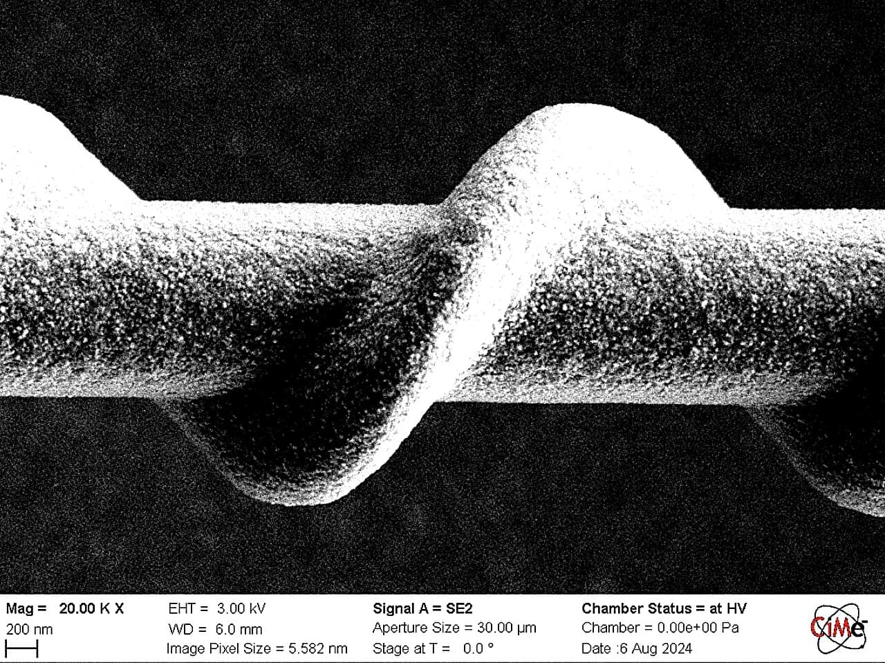
“Dirk and myself were initially inspired by the elegance of the Archimedean screw and began wondering whether we could build a magnonic analog, something that could ‘pump’ magnons (i.e., collective electron spin excitations) in a similarly directional way,” Dr. Mingran Xu, first author of the paper, told Tech Xplore.