Using lipid nanoparticle delivery of mRNAs to the liver in aged mice, T cell function and declining immune cues can be restored.
Category: nanotechnology – Page 34
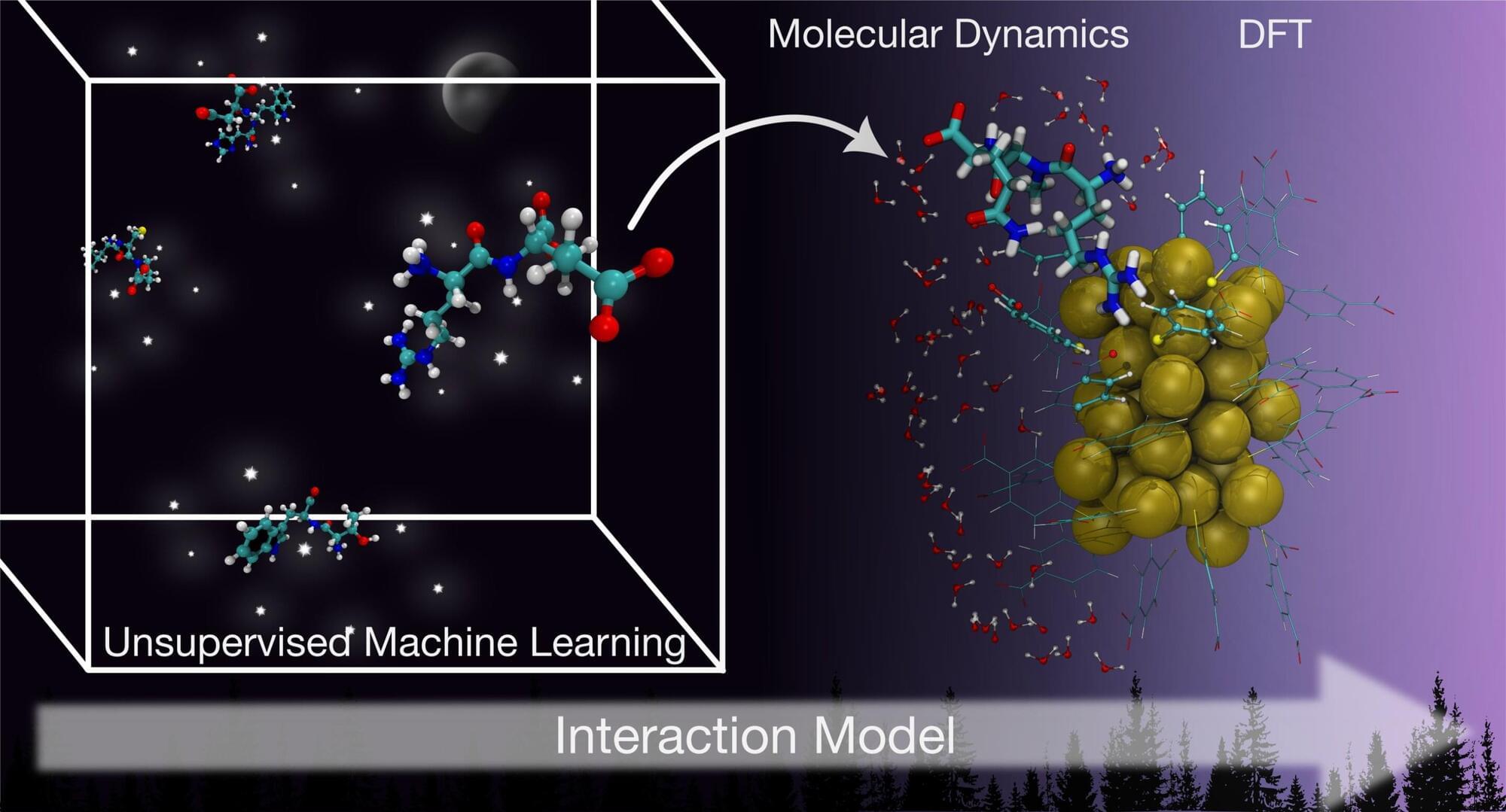
Machine learning model predicts protein binding on gold nanoclusters
Researchers in the Nanoscience Center at the University of Jyväskylä, Finland, have developed a pioneering computational model that could expedite the use of nanomaterials in biomedical applications. The study presented the first generalizable machine-learning framework capable of predicting how proteins interact with ligand-stabilized gold nanoclusters, materials widely employed in bioimaging, biosensing, and targeted drug delivery.
The adsorption of proteins onto nanomaterial surfaces is fundamental to many biological applications, including bioimaging and biosensing to targeted drug delivery. Gold nanoclusters, in particular, have attracted attention thanks to their biocompatibility and tunable optical properties. Yet existing studies that predict how proteins interact with these ligand-protected nanostructures often focus on isolated cases, leaving researchers without a unified model to guide design.
“This gap has created a clear need for general, scalable models capable of capturing the underlying rules of protein–nanocluster binding,” specifies Postdoctoral Researcher Brenda Ferrari from the University of Jyväskylä
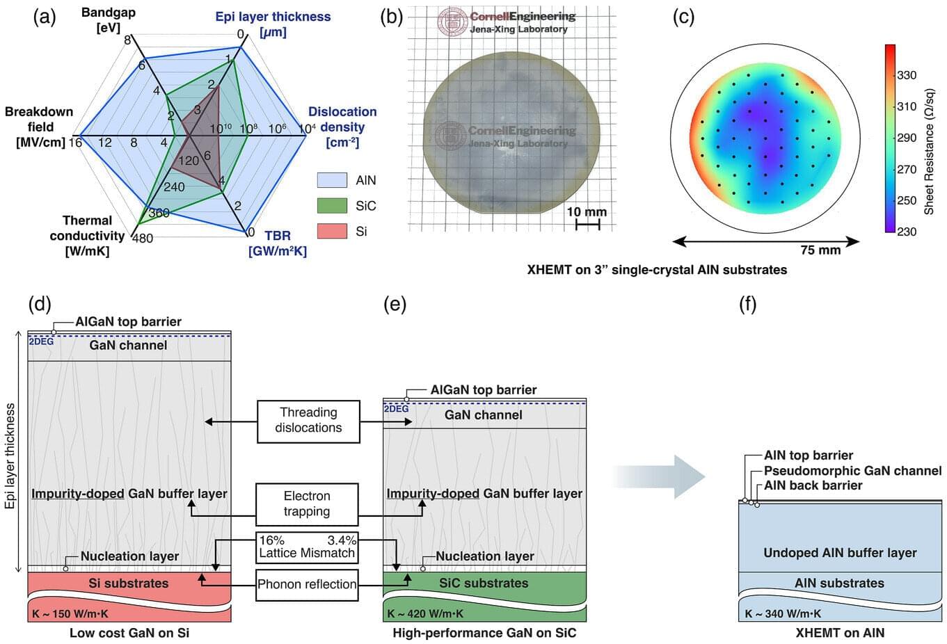
Aluminum nitride transistor advances next-gen RF electronics
Cornell researchers have developed a new transistor architecture that could reshape how high-power wireless electronics are engineered, while also addressing supply chain vulnerabilities for a critical semiconductor material.
The device, called an XHEMT, includes an ultra-thin layer of gallium nitride built on bulk single-crystal aluminum nitride, a semiconductor material with low defect densities and an ultrawide bandgap—properties that allow it to withstand higher temperatures and voltages while reducing electrical losses.
The device was detailed in the journal Advanced Electronic Materials and the research was co-led by Huili Grace Xing, the William L. Quackenbush Professor, Debdeep Jena, the David E. Burr Professor—both in the School of Electrical and Computer Engineering, the Department of Materials Science and Engineering, and the Kavli Institute at Cornell for Nanoscale Science—and doctoral student Eungkyun Kim.
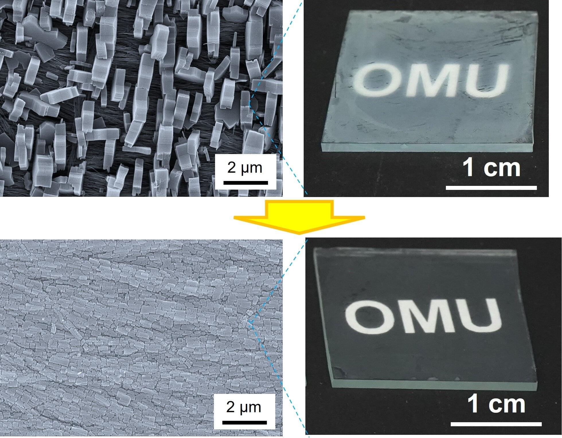
Quality control: Neatly arranging crystal growth to make fine thin films
Table salt and refined sugar look white to our eyes, but that is only because their individual colorless crystals scatter visible light. This feature of crystals is not always desirable when it comes to materials for optical and electrical devices, however.
Metal-organic frameworks are one such material. Crystalline with micropores, thin films of these nanomaterials have been attracting attention as a next-generation material that could also have an impact on environmental issues such as hydrogen storage and carbon dioxide capture.
An Osaka Metropolitan University Graduate School of Engineering team has found a way to control the growth of crystals on such thin films so that light scattering is reduced significantly.
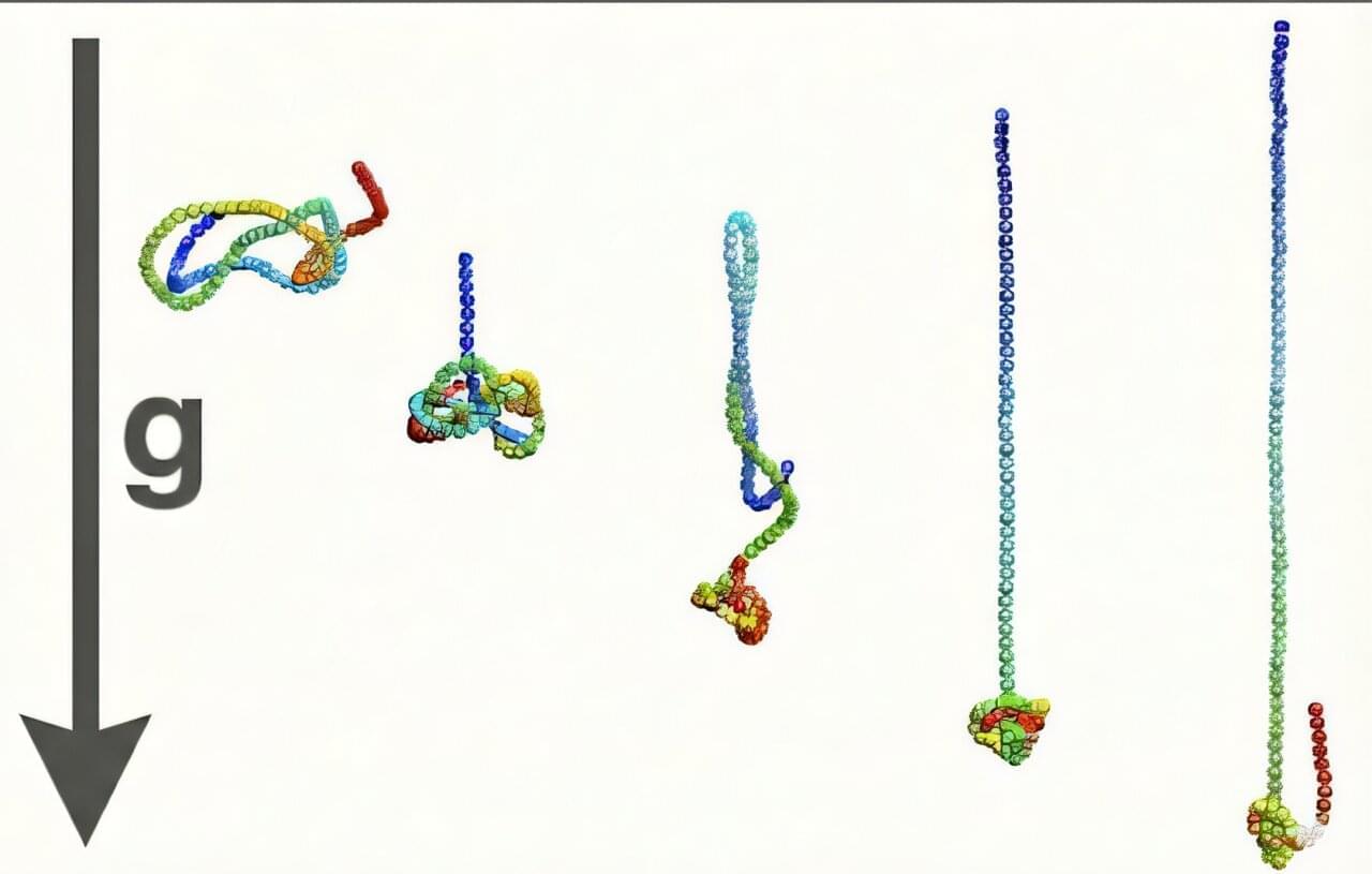
The hidden physics of knot formation in fluids
Knots are everywhere—from tangled headphones to DNA strands packed inside viruses—but how an isolated filament can knot itself without collisions or external agitation has remained a longstanding puzzle in soft-matter physics.
Now, a team of researchers at Rice University, Georgetown University and the University of Trento in Italy has uncovered a surprising physical mechanism that explains how a single filament, even one too short or too stiff to easily wrap around itself, can form a knot while sinking through a fluid under strong gravitational forces.
The discovery, published in Physical Review Letters, provides new insight into the physics of polymer dynamics, with implications ranging from understanding how DNA behaves under confinement to designing next-generation soft materials and nanostructures.
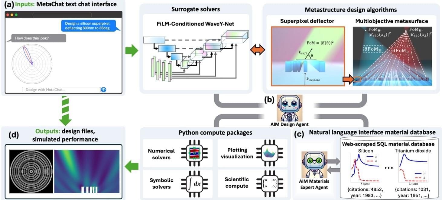
New agentic AI platform accelerates advanced optics design
Stanford engineers debuted a new framework introducing computational tools and self-reflective AI assistants, potentially advancing fields like optical computing and astronomy.
Hyper-realistic holograms, next-generation sensors for autonomous robots, and slim augmented reality glasses are among the applications of metasurfaces, emerging photonic devices constructed from nanoscale building blocks.
Now, Stanford engineers have developed an AI framework that rapidly accelerates metasurface design, with potential widespread technological applications. The framework, called MetaChat, introduces new computational tools and self-reflective AI assistants, enabling rapid solving of optics-related problems. The findings were reported recently in the journal Science Advances.
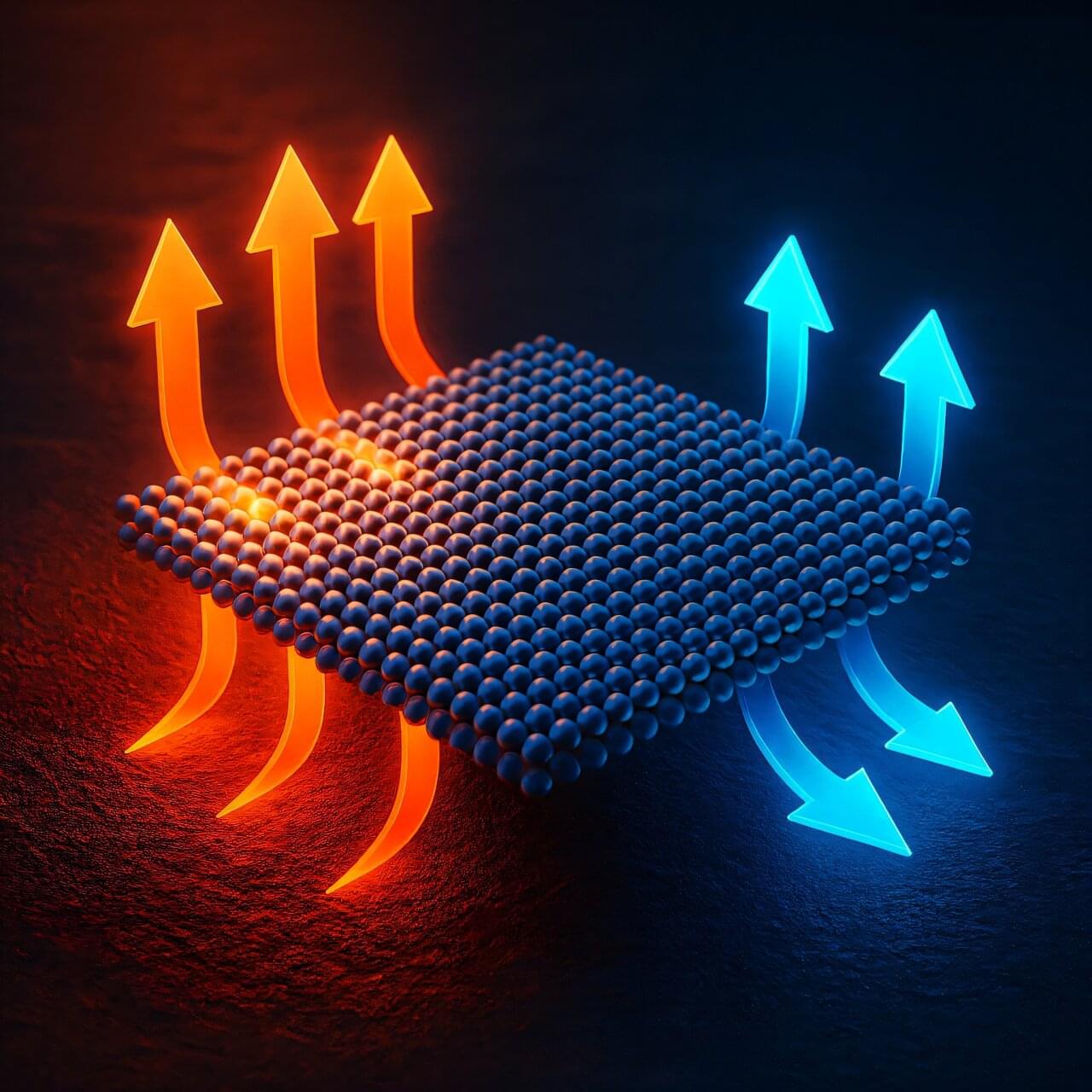
Cracking the mystery of heat flow in few-atoms thin materials
For much of my career, I have been fascinated by the ways in which materials behave when we reduce their dimensions to the nanoscale. Over and over, I’ve learned that when we shrink a material down to just a few nanometers in thickness, the familiar textbook rules of physics begin to bend, stretch, or sometimes break entirely. Heat transport is one of the areas where this becomes especially intriguing, because heat is carried by phonons—quantized vibrations of the atomic lattice—and phonons are exquisitely sensitive to spatial confinement.
A few years ago, something puzzling emerged in the literature. Molecular dynamics simulations showed that ultrathin silicon films exhibit a distinct minimum in their thermal conductivity at around one to two nanometers thickness, which corresponds to just a few atomic layers. Even more surprisingly, the thermal conductivity starts to increase again if the material is made even thinner, approaching extreme confinement and the 2D limit.
This runs counter to what every traditional model would predict. According to classical theories such as the Boltzmann transport equation or the Fuchs–Sondheimer boundary-scattering framework, reducing thickness should monotonically suppress thermal conductivity because there is simply less room for phonons to travel freely and carry heat around. Yet the simulations done by the team of Alan McGaughey at Carnegie Mellon University in Pittsburgh insisted otherwise, and no established theory could explain why.