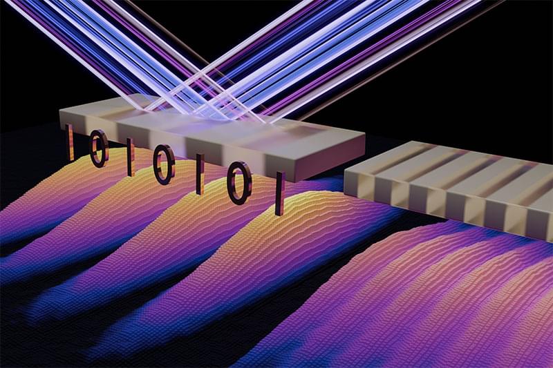
Researchers achieved high-vacuum levitation of a silica nanoparticle on a photonic-electric chip, revolutionizing nanotechnology.

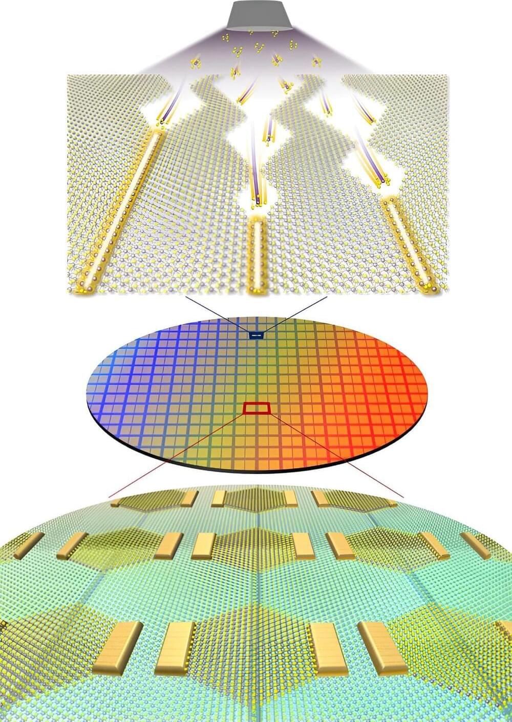
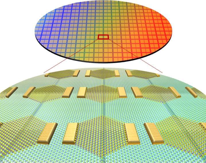
A research team led by Director Jo Moon-Ho of the Center for Van der Waals Quantum Solids within the Institute for Basic Science (IBS) has implemented a novel method to achieve epitaxial growth of 1D metallic materials with a width of less than 1 nm. The group applied this process to develop a new structure for 2D semiconductor logic circuits. Notably, they used the 1D metals as a gate electrode of the ultra-miniaturized transistor.
This research appears in Nature Nanotechnology.
Integrated devices based on two-dimensional (2D) semiconductors, which exhibit excellent properties even at the ultimate limit of material thickness down to the atomic scale, are a major focus of basic and applied research worldwide. However, realizing such ultra-miniaturized transistor devices that can control the electron movement within a few nanometers, let alone developing the manufacturing process for these integrated circuits, has been met with significant technical challenges.
A research team led by Director JO Moon-Ho of the Center for Van der Waals Quantum Solids within the Institute for Basic Science (IBS) has implemented a novel method to achieve epitaxial growth of 1D metallic materials with a width of less than 1 nanometer (nm). The group applied this process to develop a new structure for 2D semiconductor logic circuits. Notably, they used the 1D metals as a gate electrode of the ultra-miniaturized transistor.
This research was published in the journal Nature Nanotechnology (“Integrated 1D epitaxial mirror twin boundaries for ultra-scaled 2D MoS 2 field-effect transistors”).
Integrated devices based on two-dimensional (2D) semiconductors, which exhibit excellent properties even at the ultimate limit of material thickness down to the atomic scale, are a major focus of basic and applied research worldwide. However, realizing such ultra-miniaturized transistor devices that can control the electron movement within a few nanometers, let alone developing the manufacturing process for these integrated circuits, has been met with significant technical challenges.

The advent of quantum computers promises to revolutionize computing by solving complex problems exponentially more rapidly than classical computers. However, today’s quantum computers face challenges such as maintaining stability and transporting quantum information.
Phonons, which are quantized vibrations in periodic lattices, offer new ways to improve these systems by enhancing qubit interactions and providing more reliable information conversion. Phonons also facilitate better communication within quantum computers, allowing the interconnection of them in a network.
Nanophononic materials, which are artificial nanostructures with specific phononic properties, will be essential for next-generation quantum networking and communication devices. However, designing phononic crystals with desired vibration characteristics at the nano-and micro-scales remains challenging.

Luminescence refers to the result of a process in which an object absorbs light at one wavelength and then re-emits it at another wavelength. Through light absorption, electrons in the ground state of the material are excited to a higher energy state. After a certain amount of time characteristic of each excited state, the electrons decay to lower energy states, including the ground state, and emit light. The phenomenon is used in a wide array of technological applications involving highly efficient and reproducible emitting devices that can easily be miniaturized.
The materials with the highest luminescence efficiency include quantum dots (QDs), currently used in high-resolution displays, LEDs, solar panels, and sensors of various kinds, such as those used for precision medical imaging. Functionalization of the surface of QDs with various types of molecules permits interaction with cellular structures or other molecules of interest for the purpose of investigating molecular-level biological processes.
QDs are semiconductor nanoparticles whose emissive characteristics are directly linked to dot size, owing to the phenomenon of quantum confinement. For this reason, monitoring and control of crystal growth during synthesis of QDs in solution permits intelligent planning of the desired luminescence.

Machines have evolved to meet the demands of daily life and industrial use, with molecular-scale devices often exhibiting improved functionalities and mechanical movements. However, mastering the control of mechanics within solid-state molecular structures remains a significant challenge.
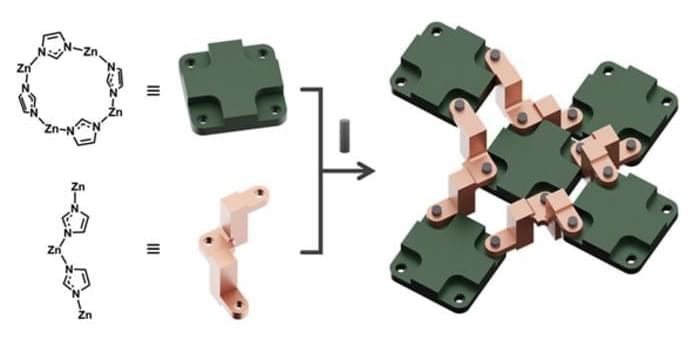
Researchers at Ulsan National Institute of Science and Technology (UNIST), South Korea have made a groundbreaking discovery that could pave the way for revolutionary advancements in data storage and beyond. Led by Professor Wonyoung Choe in the Department of Chemistry at UNIST), a team of scientists has developed zeolitic imidazolate frameworks (ZIFs) that mimic intricate machines. These molecular-scale devices can exhibit precise control over nanoscale mechanical movements, opening up exciting new possibilities in nanotechnology.
The findings have been published in Angewandte Chemie International Edition (“Zeolitic Imidazolate Frameworks as Solid-State Nanomachines”).
Magnetization can be switched with a single laser pulse. However, it is not known whether the underlying microscopic process is scalable to the nanometer length scale, a prerequisite for making this technology competitive for future data storage applications. Researchers at the Max Born Institute in Berlin, Germany, in collaboration with colleagues at the Instituto de Ciencia de Materiales in Madrid, Spain, and the free-electron laser facility FERMI in Trieste, Italy, have determined a fundamental spatial limit for light-driven magnetization reversal.
They report their finsings in Nano Letters (“Exploring the Fundamental Spatial Limits of Magnetic All-Optical Switching”).
Modern magnetic hard drives can store more than one terabit of data per square inch, which means that the smallest unit of information can be encoded on an area smaller than 25 nanometers by 25 nanometers. In laser-based, all-optical switching (AOS), magnetically encoded bits are switched between their “0” and “1” state with a single ultrashort laser pulse. To realize the full potential of AOS, particularly in terms of faster write/erase cycles and improved power efficiency, we thus need to understand whether a magnetic bit can still be all-optically reversed if its size is on the nanoscale.

Gold nanoparticles have been the subject of intense research for several decades due to their interesting applications in fields such as catalysis and medicine. “Surface ligands” are organic molecules typically present on the surface of gold nanoparticles. During synthesis, these surface ligands play an important role in controlling the size and shape of the nanoparticles.
For several decades, the CIC biomaGUNE team led by Ikerbasque Research Professor Luis Liz-Marzán has studied in detail the growth mechanisms and properties of these nanoparticles. Despite numerous advances that have recognized the importance of surface ligands, many questions remain about their exact behavior during and after growth. Direct observation of surface ligands and their interface with gold nanoparticles has therefore been a long-standing goal for many scientists in this field.
Transmission Electron Microscopy (TEM) is the technique most widely used to investigate nanoparticles. However, the study of surface ligands by means of TEM presents significant challenges; the reason is that the ligands are sensitive to the electron beam, their contrast is limited and their structure in vacuum differs from their native state in solution.