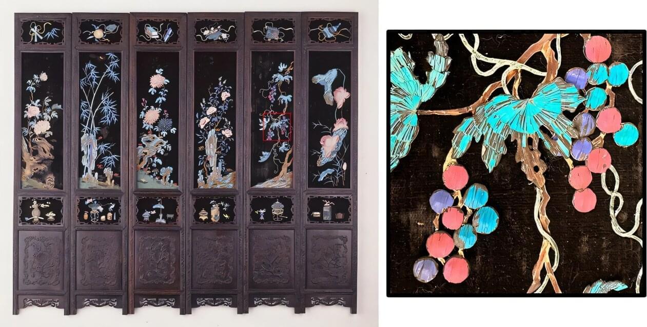
The kingfisher’s brilliant blue feathers were once used like paint to create works of art. The technique, known as tian-tsui, was popular during China’s Qing Dynasty. And because tian-tsui uses delicate feathers, previous scientists struggled to study them using traditional analytical techniques. So, researchers reporting in ACS Omega developed new methods of investigating these featherworks without harming them. The team found that multiple bird species and layered pigments provided a one-of-a-kind palette.
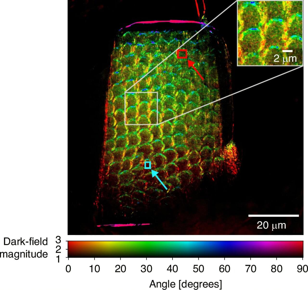
The shades of blue in kingfisher feathers are the result of a phenomenon called structural color. Rather than being created by pigment molecules, structural color is created by tiny, ordered structures in the feathers that interact with light to create the observed coloring—in this case, blue or purple. To gain insights into several featherwork pieces and the feathers that went into making them, Madeline Meier and colleagues combined different imaging and spectroscopy techniques that rely on the ways the feathers reflect and scatter light.
The team analyzed a decorative tian-tsui screen estimated to date from the late 18th to the early 19th century that features intricate scenes in a variety of colors. In one panel, analysis revealed that the blue feathers belonged to the common kingfisher, and the purple came from the black-capped kingfisher. The green feathers had different nanostructures than the blue feathers, leading the researchers to conclude that the green ones belonged to another bird entirely: the mallard duck.